

HDI_PCB Yang's Store
Owned by HDI_PCB Yang Joined Mar 2024 18 Listings
HDI_PCB Yang's Store
easyid.me/biz/hdi-pcb-leah-e0ece9 • Verified Store
Scan to open official EasyID digital store, view live catalog, or save business card.
Verified Merchant
EasyID Certified Seller
Fast 24h Packing
Direct courier dispatch
Zero Escrow Direct
Direct merchant settlement
Store Listings (18)
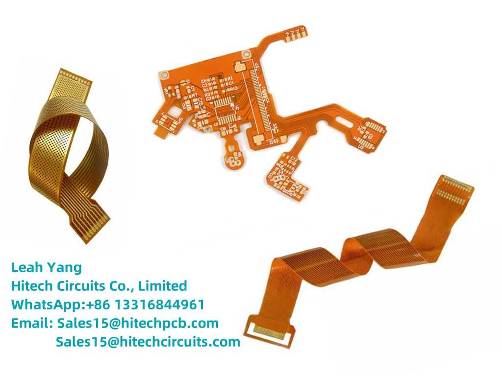
Fabricante y Ensamblaje de PCB Flexible - Servicios Integrales Para el ensamblaje SMD en la PCB flexible, el posicionamiento exacto y la fijación de la PCB flexible son los puntos clave, y la clave de la fijación es hacer la placa de soporte adecu...
Para el ensamblaje SMD en la PCB flexible, el posicionamiento exacto y la fijación de la PCB flexible son los puntos clave, y la clave de la fijación es hacer la placa de soporte adecuada; En segundo lugar está el pr - horneado, impresión, parche y soldadura por reflujo de la PCB flexible, obviamente, el proceso SMT de la FPC es más difícil que la PCB rígida, por lo que es necesario establecer con precisión los parámetros del proceso y la estricta gestión del proceso de producción también es importante. Es necesario asegurarse de que los operadores apliquen estrictamente cada regla de SOP, los ingenieros y IPQC deben reforzar la inspección, y descubrir las condiciones anormales de la línea de producción a tiempo, analizar las causas y tomar las medidas necesarias, a fin de controlar la tasa de defectos de la línea de producción.
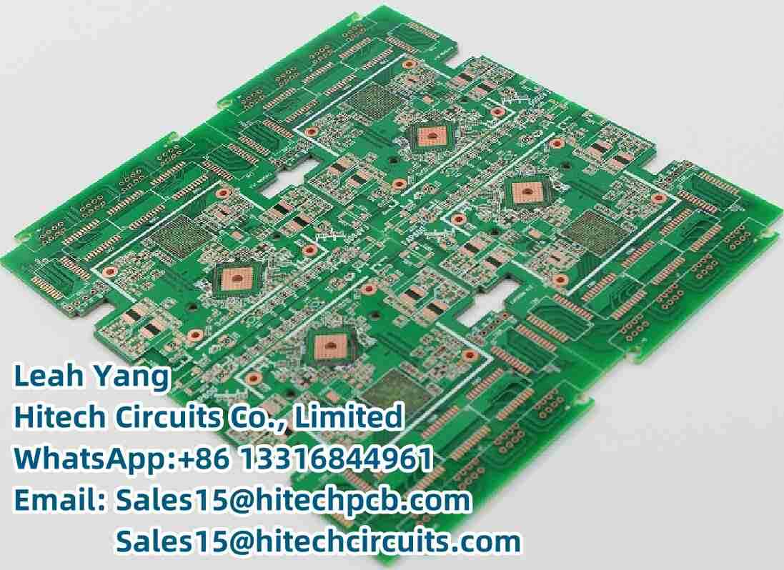
¿Qué es una PCB HDI?
Las placas de circuito impreso de interconexión de alta densidad (HDI) se caracterizan por líneas más finas, espacios más estrechos y cableado más denso, lo que permite una conexión más rápida al tiempo que reduce el tamaño y el volumen de un proyecto. Estas placas también incorporan vías ciegas y enterradas, microvías ablacionadas por láser, laminado secuencial y pasamuros. <br> <br>Como resultado, una placa HDI puede albergar la funcionalidad de las placas anteriores utilizadas. HitechPCB es un fabricante y proveedor de PCB HDI en Shenzhen,Chinasupports HDI PCB prototipo y producción en masa con precio menos costoso y rápido tiempo de entrega. Los clientes de una variedad de industrias que servimos tienen en común que tienen altas expectativas en calidad, fiabilidad y entrega a tiempo en la producción de PCB HDI. Nuestra calidad no es una ocurrencia tardía, sino que está integrada en cada proceso, desde la fase inicial hasta la fabricación y el envío. <br> <br>Las placas de circuitos impresos de HDI se desarrollaron a partir de la necesidad de proporcionar un mayor nivel de potencia y rendimiento computacional en una envoltura más pequeña. Esta necesidad fue impulsada en gran medida por sectores como el de las telecomunicaciones, en el que la necesidad de ofrecer teléfonos móviles más pequeños y potentes exigía encontrar una forma de empaquetar más circuitos electrónicos en un envoltorio más pequeño y denso. Sin embargo, otros factores clave para el desarrollo de las placas de circuito impreso de alta densidad fueron las tendencias en la tecnología de circuitos integrados (CI), que obligaron a reconsiderar el diseño de las interconexiones y la disposición de las placas de circuito impreso. Algunas de estas tendencias clave de la tecnología de CI son <br> <br>Ventajas de Placas de Circuito Impreso HDI <br> <br>La tecnología HDI ofrece varias ventajas y beneficios a diseñadores e ingenieros. <br>Diseño compacto - Las placas HDI tienen una gran capacidad de cableado y pueden reducir tanto el tamaño como el número de capas necesarias para producir un diseño frente al uso de las placas de circuito impreso tradicionales. <br> <br>El uso de microvías y de la tecnología "via in pad" permite colocar los componentes más cerca unos de otros y montar más componentes en un solo lado de la placa, lo que se traduce en una transmisión de señales más rápida y en una mejora de la integridad de la señal gracias a trayectos de señal más cortos. <br> <br>El taladrado por láser produce orificios más pequeños y mejora la resistencia térmica de la placa. <br> <br>La posibilidad de reducir el número de capas necesarias en el diseño de PCB puede reducir los costes. <br> <br>Se pueden admitir dispositivos de paso bajo, como los BGA, cuyo paso puede ser de 1 mm o menos. <br> <br>La menor relación de aspecto en las vías de HDI mejora el chapado de las vías y la fiabilidad general de la placa. <br> <br>Aplicaciones de las placas de circuito impreso HDI <br> <br>Las placas de circuito impreso de HDI han permitido empaquetar más componentes electrónicos en un sobre más pequeño, ayudando a reducir el tamaño de los productos en varios mercados. Algunos ejemplos de aplicaciones de PCB de DHI son: <br> <br>Sanidad y medicina – dispositivos implantados como marcapasos cardíacos y dispositivos externos como audífonos. <br>Industria automovilística – dispositivos electrónicos más pequeños y ligeros que ahorran espacio y reducen el peso del vehículo. <br>Dispositivos de consumo – teléfonos móviles, tabletas, ordenadores portátiles y productos con pantalla táctil han reducido su tamaño y peso con un mayor rendimiento gracias a la tecnología HDI. <br> <br>Aeroespacial – los diseños electrónicos para sistemas de misiles, aeronaves y aplicaciones de defensa utilizan placas de circuitos impresos HDI que proporcionan un funcionamiento fiable en condiciones ambientales extremas.
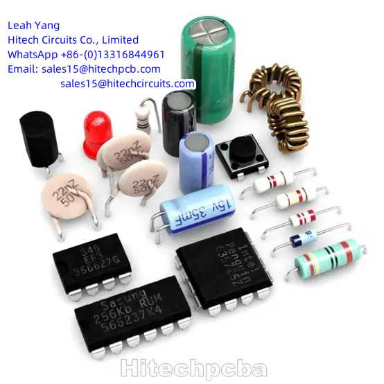
Compra de Componentes Compra de Componentes, proveedor de piezas electrónicas - Hitech Circuits Co., Limited
¿Qué es Compra de Componentes? <br> <br>Servicio de agriado de componentes (piezas electrónicas) Hitech Circuits es una empresa de fabricación, ensamblaje y diseño de PCB. Al elegir nuestro servicio de ensamblaje de PCB llave en mano, todos los componentes electrónicos, incluyendo las partes activas y pasivas serán proporcionados por nosotros. Esto significa que somos responsables de la compra de componentes BOM. Somos conscientes de la importancia de reducir el coste de los componentes y acortar los plazos de fabricación de PCB y PCBA mediante la gestión estratégica de la compra de componentes. Gracias a nuestras relaciones de trabajo a largo plazo con muchos fabricantes y distribuidores de componentes tanto nacionales como extranjeros, podemos adquirir piezas difíciles de encontrar a buenos precios y plazos de entrega, y ofrecerles una amplia gama de componentes de calidad. Todos los proveedores de componentes son auditados por pasar nuestras normas de calidad y el requisito de tiempo de entrega de abastecimiento, y sólo las fuentes de confianza se les permite la adquisición y aplicación en sus proyectos de ensamblaje de PCB no importa en prototipos, de bajo volumen y grandes volúmenes. <br> <br>Tiras y Cintas Continuas para Consignación o Ensamblaje Parcial Llave en Mano La correcta configuración y funcionamiento de la máquina SMT requiere que las piezas sobren (o sobran) porque hay una pequeña longitud entre el alimentador y la boquilla de recogida de la máquina de colocación no se puede utilizar. En el proceso de recogida y colocación, la máquina puede desechar algunas piezas, y las piezas electrónicas que se cargan en los alimentadores pueden perderse de forma manual. Las piezas no utilizadas y excesivas suministradas por usted o adquiridas por nosotros serán empaquetadas y devueltas a usted junto con el ensamblaje de la placa de circuito impreso. Las piezas SMT que no se suministran en bobinas deben estar en una tira continua de cinta. Si necesita ensamblar diferentes placas de circuito impreso con las mismas piezas SMT, no las corte en más tiras, manténgalas en la tira continua de la cinta o en los carretes. Estándar de cantidad de compra de componentes o cantidad suministrada para prototipos de ensamblaje de PCB como la tabla en Exceso de componentes y cantidades. Para grandes volúmenes de ensamblaje de PCB, Hitechpcb puede suministrar un porcentaje de piezas adicionales. Todas las piezas adicionales son necesarias para garantizar un ensamblaje sin problemas y el envío de sus placas ensambladas a tiempo sin escasez. <br> <br>Suministro De Componentes - Suministro De Piezas Electrónicas - Hitech Circuits (hellopcba.com)
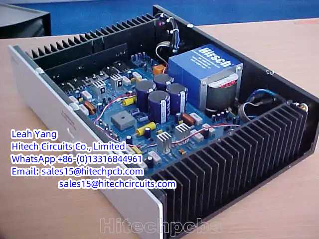
Ensamblaje Completo de Caja de PCB
¿Qué es ensamblaje en caja de PCB? <br> <br>Los montajes en caja, también conocidos como integración de sistemas, pueden ser desde simples PCBA (componentes de placa de circuito impreso) montados en pequeñas cajas hasta armarios que albergan complejos sistemas electromecánicos. El ensamblaje en caja implica el diseño, la producción y la construcción de todos los enlaces. <br> <br>El ensamblaje completo incluye todos los demás trabajos de montaje que intervienen en el ensamblaje electromecánico, a excepción de la producción de placas de circuitos impresos. La construcción de cajas a veces se llama "integración de sistemas". <br> <br>Construir cajas significa diseñar y fabricar armarios, ensamblar PCBA, montar conjuntos de cables y mazos de cables e incluso instalar sistemas eléctricos y/o neumáticos. Hitechpcba Manufacturing ofrece una gama completa de servicios que incluyen el embalaje, el etiquetado y el envío hasta su ubicación. <br> <br>Construcción de cajas Servicio y proceso de ensamblaje <br> <br>Muchos clientes son fabricantes y no sólo necesitan el ensamblaje de circuitos impresos, sino también el montaje final de productos innovadores. <br> <br>La "construcción de cajas", también conocida como integración de sistemas, es el ensamblaje completo del producto final del cliente. El proceso va más allá de la producción de PCB (PCB) y abarca el ensamblaje electromecánico, incluida la fabricación de cajas, la instalación y el tendido de cables o mazos, y la instalación de subconjuntos y ensamblajes. Una caja puede referirse al ensamblaje de PCB (PCBA) en un armario lleno de cables, una pequeña caja o un complejo sistema electromecánico totalmente integrado con neumática y electrónica. <br> <br>Estos ensamblajes de cajas incluyen los siguientes componentes: <br> <br>ensamblaje del producto <br> <br>ensamblaje a nivel de sistema <br> <br>Ensamblaje de segmentos de producto <br> <br>embalaje y etiquetado <br> <br>prueba <br> <br>Carga de software y configuración del producto <br> <br>Servicio posventa <br> <br>Almacenamiento y trazabilidad <br> <br>Estamos orgullosos de ofrecer soluciones llave en mano para todas sus necesidades de subcontratación. Nuestro negocio de ensamblaje de cajas finales ha crecido para satisfacer las necesidades de nuestros clientes con soluciones completas. Podemos abastecernos de todos los materiales necesarios, construir los PCBA, suministrar los cables necesarios y completar el proceso de fabricación construyendo el producto final del cliente. <br> <br>En Hitech Circuits, liberamos a nuestros clientes para que puedan centrarse en otros aspectos de su negocio. Nuestros servicios ayudan a las empresas a reducir la necesidad de invertir en capital interno y otros recursos. <br> <br>Nuestro equipo especializado en la construcción de cajas puede realizar ensamblajes desde pequeños y sencillos hasta grandes y complejos. Póngase en contacto con nosotros hoy mismo para obtener un presupuesto gratuito para su próximo trabajo de construcción de cajas. <br> <br>Ensamblaje Completo De Cajas De Pcb (hellopcba.com)
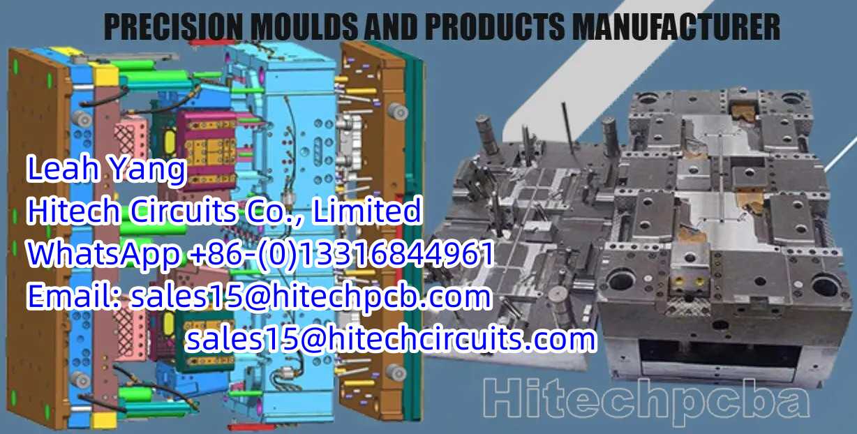
Moldeo De Plástico
¿Qué es Moldeo de Plástico? <br> <br>Es importante que entienda qué es exactamente el moldeo de plástico, y cómo puede beneficiar a su negocio, el moldeo de plástico es el proceso de utilizar una máquina de moldeo de plástico y un molde de plástico para crear productos de plástico. <br> <br>Esencialmente, el material plástico entra en el barril de calentamiento, el barril de calentamiento tiene una temperatura de hasta 280-320 grados para fundir el material plástico en un líquido, que luego se mezcla y se fuerza en una cavidad del molde. A continuación, enfriar el molde y obtener el plástico afilado lo que quiere, Se utiliza para algunos de los componentes pequeños o grandes que usted quiere tener en sus productos finales. <br> <br>Piezas de plástico moldeado podría ser una parte de su nuevo modelo, si usted está haciendo el desarrollo de nuevos productos, entonces usted necesitará piezas de plástico moldeado en todo su negocio. <br> <br>Si necesita piezas específicas para su negocio, primero tiene que encontrar un fabricante de moldeo de plástico y una empresa de moldeo de plástico. Y nosotros somos el que podría resolver su problema en moldeo de plástico y piezas moldeadas. <br> <br>Hay varios tipos de procesos de moldeo de plástico como a continuación, para entender esto tal vez le ayudará a desarrollar su proyecto y encontrar el mejor proceso para hacer el mejor resultado. <br> <br>El moldeo por inyección de plástico es una técnica utilizada para moldear plástico con la forma del objeto que se desea producir. Durante el proceso de moldeo por inyección, se inyectan polímeros termoplásticos en la cavidad de un molde. Para ello, se calientan gránulos de un material para que puedan inyectarse en la cavidad en estado líquido. A continuación, este líquido caliente se deja enfriar en el molde para que la pieza pueda fraguar correctamente. Una vez que se expulsa una pieza del molde, puede iniciarse inmediatamente otro ciclo. <br> <br>Aunque el moldeo por inyección también puede utilizarse para metales y vidrio, es un proceso de producción especialmente popular para la fabricación de piezas de plástico. <br> <br>Los pasos de un ciclo de proceso de moldeo por inyección incluyen la sujeción, la inyección, el enfriamiento y la expulsión. <br> <br>Durante la sujeción, el molde de inyección se prepara para un ciclo sujetando firmemente las dos mitades que forman la cavidad del molde. Esto garantiza que la pieza moldeada tenga un aspecto liso y lo ideal es que la pieza moldeada no tenga casi ninguna línea donde se juntan las diferentes mitades, ya que esto indica que el molde podría no estar sujetándose lo suficientemente fuerte. <br> <br>Una vez unidas las mitades del molde, éste está listo para formar una pieza. Antes de inyectar el polímero en el molde, los gránulos se calientan para formar un líquido. A continuación, el polímero líquido se inyecta en el molde a través de una boquilla. Esta es la etapa de inyección del proceso de moldeo, que es la segunda etapa de un ciclo de cuatro etapas. <br> <br>A continuación, la pieza se deja enfriar en el molde durante un tiempo predeterminado. La etapa de enfriamiento puede durar desde unos segundos hasta unos minutos, dependiendo del polímero que se utilice para producir la pieza. Mientras que algunos polímeros apenas necesitan tiempo para enfriarse, otros pueden tardar unos minutos. Todo depende de la pieza que se fabrique. <br> <br>Moldeo De Plásticos (hellopcba.com)
Servicios de Fabricación Electrónica China EMS proveedor - Hitech Circuits
Servicios de Fabricación Electrónica <br> <br>Servicios De Fabricación Electrónica - Ems Fabricación De Placas De Circuito Impreso (hellopcba.com) <br> <br>Hitech Circuits siempre se ha centrado en los servicios de fabricación electrónica durante más de 15 años con mucha experiencia para el diseño y la producción en el campo de PCBA. Proporcionamos servicios de ventanilla única, incluyendo montaje SMT, plug-in (THT), adquisición y aprovisionamiento de componentes electrónicos, ensamblaje de productos acabados, pruebas y otros servicios integrales. <br> <br>Desde la introducción de nuevos productos hasta el suministro de componentes personalizados, pasando por una producción estable, proporcionamos soluciones para todo el ciclo de vida del producto, lo que permite a nuestros clientes alcanzar el éxito. Hitech Circuits crea valor para los clientes a través de servicios avanzados de ingeniería de valor, soluciones de componentes personalizados, disposición global de la fábrica y gestión de alto nivel de la cadena de suministro. <br> <br>Hemos introducido avanzados equipos importados de producción y pruebas, y llevamos mucho tiempo comprometidos con el desarrollo de nuevas tecnologías, aplicando una exhaustiva gestión de la calidad y del medio ambiente. Por todo ello, nos hemos convertido en un líder del sector con precios muy competitivos, productos de gran estabilidad, garantía de entrega fiable y un servicio excelente. <br> <br>En HITECH CIRCUITS, podemos satisfacer todas sus necesidades de fabricación rápida de PCB. <br> <br>Contacte con nosotros, Email add: [email protected] <br> <br>Servicios De Fabricación Electrónica - Ems Fabricación De Placas De Circuito Impreso (hellopcba.com)
Rigid-flex PCB manufacturer up to 18 layers
What are Rigid-Flex Circuit Boards? <br> <br>As the name implies, a Rigid-Flex PCB is a hybrid of a Flex PCB and a Rigid PCB. The combination of the two types of boards utilises the benefits each one provides, integrating the versatility of the flexible board with the robustness of the rigid board. Rigid-flex printed circuit boards are used in more complex mechanical designs, eliminating flexible cables and wiring and replacing it with integrated circuits. <br> <br>Rigid-Flex PCBs, by definition, are a combination of rigid part(s) joined by interconnecting flex areas where the flex material is used across the entire PCB area. <br> <br>The rigid parts are where there is no bending requirement. Again, PTHs take connections from layer to layer as required. Rigid-flex may also employ other technologies as required eg. HDI. Unlike the cost-effective flex PCBs, Rigid-Flex PCBs can be a bit more costly due to their intricate design. <br> <br>Rigid-flex PCB design can be used to eliminate or greatly reduce requirements for bulky and costly cable harnesses, in turn taking out costs and reducing assembly time. Like the pure flexible PCBs, a high volume of rigid-flex PCBs are used in aviation and space applications – and also in automotive and test equipment. <br> <br>The flexible layers of a Rigid-Flex PCB are buried within the board and penetrate through the rigid sections of the PCB. <br> <br>The trend to miniaturization in electronics continues. Integrated circuit board solutions are becoming more and more popular as a means of efficiently utilizing the even smaller casing volume in all three dimensions. <br> <br>A rigid-flex printed circuit board is unique as the rigid part of the circuitry can be placed directly into the application. Then, the flexible section can be bent and even folded to fit around components to make another direct connection. This aspect ensures a reliable connection to parts for higher performance. <br> <br>Some of the most common products that incorporate rigid-flex PCBs in their design include laptop computers, smartphones, and wearable devices due to the bending capabilities of rigid-flex. <br> <br>Rigid-flex pcb boards are PCBs that have Flexible PCBs (FPC) and Rigid PCBs on the same board, which are commonly employed to save space, remove wiring assemblies and can also be welded with complex components. Combining other higher technology boards, such as HDI, as a part of its packaging, is also a common design. <br> <br>Rigid Flex PCB design <br> <br>The designs of Rigid Flex PCBs are a little more complex as these boards are designed in 3D, which allows the board to be folded or twisted to create the desired shape for the product. Designing a board in 3D means they can offer greater spatial efficiency and can subsequently be used in special instances where space and weight reduction may be necessary, such as in medical devices. By being able to design in three dimensions designers can twist, fold and roll the flexible board substrates to achieve their desired shape for the final application's package. <br> <br>Rigid Flex PCBs are usually thinner than other boards, meaning it’s a great option for any thin or light packaging needs your products may have. With thin copper layers and adhesive-less laminates, it’s a great small, thin and light solution for your circuit design needs. <br> <br>Rigid-Flex PCBs Fabrication Applications: <br> <br>Rigid-Flex PCBs offer a wide array of applications, ranging from smart devices to cell phones and digital cameras. Increasingly, rigid-flex board fabrication has been used in medical devices such as pacemakers for their space and weight reduction capabilities. The same advantages for rigid-flex PCB usage can be applied to smart control systems. <br> <br>In consumer products, rigid-flex doesn't just maximize space and weight but greatly improves reliability, eliminating many needs for solder joints and delicate, fragile wiring that are prone to connection issues. These are just some examples, but Rigid-Flex PCBs can be used to benefit nearly all advanced electrical applications including testing equipment, tools and automobiles. <br> <br>Rigid-Flex PCB and Its Production Process <br> <br>The development of FPC and PCB has spawned a new product that is called rigid-flex PCB. Therefore, rigid- flex PCB is according to the relevant process requirements and through the lamination process to combine rigid board and flex board to form a circuit board with FPC characteristics and PCB characteristics. <br> <br>Because rigid-flex PCB has a variety of complex structural forms, the manufacturing process is also different. Below picture shows the regular rigid-flex PCB and an example for regular stack up design. <br> <br>Rigid flex PCB production is based on below steps: the first step is to process the rigid outer cover layer. The electroplating graphic that needs to be pressed in the outer layer, and then through the CNC milling machine, punching or laser method, routing out or routing the half of depth of the flexible part which is located in rigid layer. Flex board and the rigid outer cover are boned by adhesive sheet. The adhesive sheet has been pre-opened in the flexible part. <br> <br>During the lamination process, if the rigid outer layer uses routing structure, a suitable pressure filling board should be prepared for the flex part. Using a vacuum pressing machine to obtain better press quality, and meanwhile with some auxiliary coating materials, such as PE, etc., so that the pressing process can provide a uniform pressure on the entire board, and make the low -flowing sticky sheet is fully flowing and filling the gap, especially for complex structures. Before adhesion or lamination, appropriate baking should be done as needed to remove moisture. <br> <br>After lamination, the rigid- flex PCB can use a through hole treatment process which is similar to a multi-layer rigid board, the different part is remove drilling dirt. The method of removing drilling dirt depends on what materials used. Like the rigid board, drilling the hole after fully baking, and then use the plasma etching process to remove the residue in the hole wall. Before the plasma is treated, bake is also needed to remove water vapor. Caval polyesterness is generally recommended to not exceed 13um. The pore -plating process of conventional rigid board can be used, but the specific process parameters of the electroplating should be determined according to the reliability test data of the pores. <br> <br>The next process is similar to the multi -layer rigid board. The outer layer etching, covering membrane (welded film), surface treatment, etc. can be used in similar processes. When making outline of the rigid-flex PCB, remove the filling board in the flexible part or depth control rigid outer cover in the flexible area can be formed into a rigid-flex PCB. <br> <br>Careful consideration of Rigid-Flex solutions and a proper assessment of the available options at the early stages in the rigid-flex PCB design phase will return significant benefits. The Rigid-Flex PCBs fabricator must be involved early in the design process to ensure the design and fab portions are both in coordination and to account for final product variations. <br> <br>The Rigid-Flex manufacturing phase is also more complex and time-consuming than rigid board fabrication. All the flexible components of the Rigid-Flex assembly have completely different handling, etching, and soldering processes than rigid FR4 boards. <br> <br>Benefits of Rigid Flex PCB <br> <br>Space requirements can be minimized by applying 3D <br> <br>By removing the need for connectors and cables between the individual rigid parts the board size and overall system weight can be reduced. <br> <br>By maximizing space, there is often a lower count in parts. <br> <br>Less solder joints assure higher connection reliability. <br> <br>Handling during assembly is easier in comparison with flexible boards. <br> <br>Simplified PCB assembly processes. <br> <br>Integrated ZIF contacts provide simple modular interfaces to the system environment. <br> <br>Test conditions are simplified. A complete test prior to installation becomes possible. <br> <br>Logistical and assembly costs are significantly reduced with flex-rigid boards. <br> <br>It is possible to increase the complexity of mechanical designs, which also improves the degree of freedom for optimized housing solutions. <br> <br>Rigid Flex PCB Fabrication Applications <br> <br>Rigid flexible PCBs offer a wide array of applications, ranging from military weaponry and aerospace systems to cell phones and digital cameras. Increasingly, rigid flex board fabrication has been used in medical devices such as pacemakers for their space and weight reduction capabilities. The same advantages for rigid flex PCB usage can be applied to military weaponry and weapon control systems <br> <br>In consumer products, rigid flex doesn't just maximize space and weight but greatly improves reliability, eliminating many needs for solder joints and delicate, fragile wiring that are prone to connection issues. These are just some examples, but rigid flex PCBs can be used to benefit nearly all advanced electrical applications including testing equipment, tools and automobiles. <br> <br>Available structures for rigid flex PCB <br> <br>There are numerous, different structures available. The more common ones are defined below: <br> <br>Traditional rigid flex construction (IPC-6013 type 4) Multilayer rigid and flexible circuit combination containing three or more layers with plated through holes. <br> <br>Asymmetrical rigid flex construction, where the FPC is situated on the outer layer of the rigid construction. Containing three or more layers with plated through holes. <br> <br>Multilayer rigid flex construction with buried / blind via (microvia) as part of the rigid construction. 2 layers of microvia are achievable. Construction may also include two rigid structures as part of a homogeneous build. <br> <br>Rigid Flex Printed Circuit Board Manufacturer <br> <br>Rigid flex printed circuit boards (PCBs) are manufactured by combining rigid and flexible board technologies. These circuit boards are made up of multiple flexible circuit inner layers. An epoxy pre-preg bonding film is used to attach together these inner layers. The key benefit of these boards is that they are a combination of the best quality of flexible and rigid circuit boards. This can have several further benefits as far as stability, assembly, signal transmission, and overall size of the circuit are concerned. Hitechpcb provides a number of variants in rigid flex PCBs, which include 4 layer rigid flex with ENIG finish, 10 layer rigid flex with 4 layer flex, 12 layer rigid flex with heat sink, 14 layer rigid flex circuit boards, and many more. It is one of the leading rigid flex PCB manufacturers. <br> <br>Every printed circuit board depends on the copper for carrying electricity. We understand that copper thickness plays a key role in the performance of these circuit boards. Thus, we allow the customers to choose from a variety of copper thicknesses, including 0.5 OZ, 1.0 OZ, 2.0 OZ, 3.0 OZ, up to 6 OZ. The solder mask helps in improving the aesthetic appeal of the components on the PCB. We can provide rigid flex printed circuit boards in various solder mask colors, including white, black, blue, green, red, and Taiyo PSR4000 white. The PCB can be availed in silkscreen colors – black and white. <br> <br>Rigid flex printed circuit boards have minimal space requirements that are optimized by 3D application. These circuit boards require no cables or connectors between the rigid parts. This helps reduce the board size, as well as overall system weight. These lesser solder joints also help assure high connectivity. Additionally, these boards have ZIF contacts that are integrated. These contacts help simplify the system interfacing. This 4 layer rigid flex PCB and other printed circuit boards are vacuum packed during the transit. This helps us assure the quality, as well as working condition of the boards. <br> <br>The Disadvantage and Advantage of Rigid-Flex PCB <br> <br>Rigid-flex PCB has many production processes with the characteristic of superior difficulty in production and high defect rate. Its biggest disadvantage is that the price is more expensive than flex PCB or rigid PCB and long production cycle. Another disadvantage is that both SMT and furnaces may need to use carrier to support the flex PCB which virtually increases the SMT cost. <br> <br>One of the key features of rigid-flex PCB is the thin profile and changeable shape, making it an ideal solution for ultra -thin and ultra -light packaging. Although the rigid flex PCB may be more expensive in design and manufacturing, they do have many advantages and can solve many problems in traditional hardboard technology. <br> <br>1. Small Size and Flexible Shape <br> <br>The rigid- flex PCB is easier to install more components in smaller space, because they can change the shape according to a specific contour. This technology will reduce the size and weight of the final product and the overall system cost. At the same time, the compact shape of rigid flex PCB makes it the best choice for fine lines and high -density circuits in HDI technology. <br> <br>2. Customized for Different Applications <br> <br>Rigid-flex PCB has various packages, which can be customized for the application of many industries such as aerospace, military, medical equipment and consumer electronics. They can customize the size and shape to adapt to the shell design and 3D design, which provides designers with more possibilities to meet different requirements in specific applications. <br> <br>3. Better Mechanical Stability <br> <br>The stability of the rigid board and the flexibility of the flexible board form the stable structure of the entire packaging, while retaining the reliability and flexibility required for small space installation. <br> <br>4. Good Performance in Harsh Environments <br> <br>Rigid-flex PCB has high resistance and high vibration capacity, so they can work normally in a high -stress environment. There are fewer cables and connectors used in rigid-flexible PCB, which also reduces security risks and maintenance in future use. <br> <br>5. Easy to Manufacture and Test <br> <br>The rigid-flex PCB requires a small number of inter connect and related components/parts. It helps simplify the assembly operation, making rigid –flex PCB easier to assemble and test. Rigid-flex PCB is very suitable for PCB prototypes. <br> <br>In addition to the above advantages, other common advantages of rigid-flex PCB also include high circuit density, good heat dissipation and good chemical resistance. In a word, rigid-flex PCB combines all the advantages of rigid PCB and flex PCB, and at the same time make up for the shortcomings. This PCB is the best solution to design reliable and powerful circuits for smart wearable devices and other industries. <br> <br>[a]https%3A%2F%2Fwww.hitechpcba.com%2Frigid-flex-pcb-manufacturer[/a]
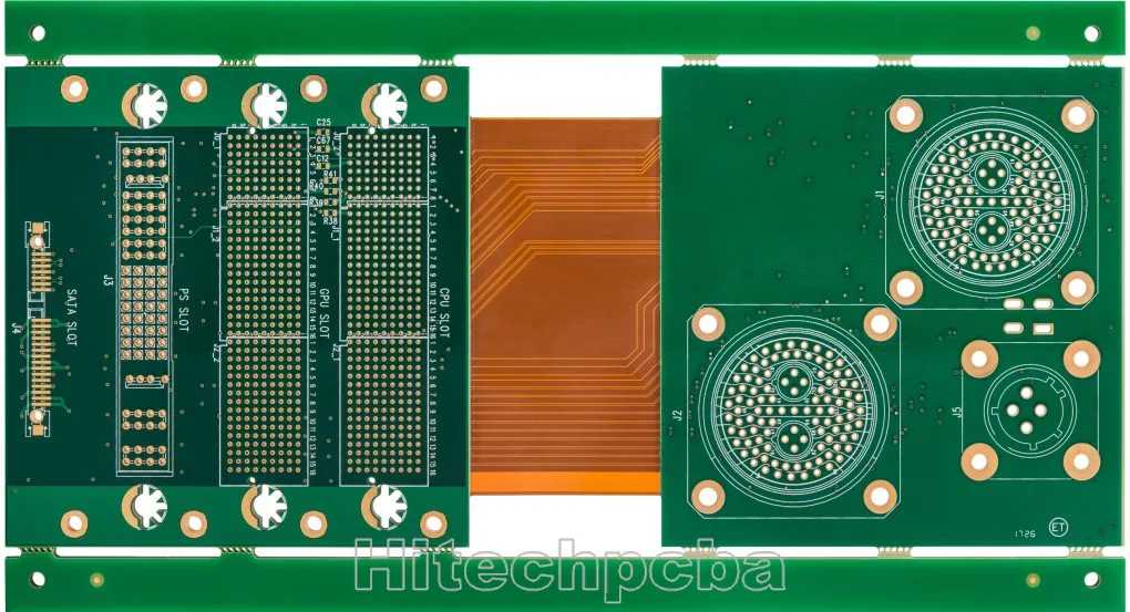
Rigid flex pcb board
What is rigid flex pcb board? <br> <br>Rigid-flex PCB board, it is a circuit board that combines flexible and rigid circuit board technology in the application. Most rigid-flex boards are composed of multiple layers of flexible circuit boards, which are attached to one or more rigid boards from the outside and/or from the inside, depending on the design of the application. The flexible substrate is designed to be in a constant deflection state, and is usually formed as a deflection curve during rigid flex pcb manufacturing or assembly. <br> <br>Hitech rigid flex pcb manufacturing process <br> <br>After the production of FPC flexible boards is completed, the production of Hitech rigid flex pcb boards can be completed through the following processes. <br> <br>1. Punching <br> <br>Drill holes on FR4 and PP film, and the design on the alignment hole is not the same as the general through hole. After the punching is completed, browning is required. <br> <br>2. Riveting <br> <br>Laminate copper clad laminates, PP adhesives, and FPC circuit boards and place them neatly. The original old process is to laminate and pressing step by step, but it is a waste of time. After many attempts, we found that the stacking process can be completed once. <br> <br>3. Laminate <br> <br>This is a relatively complete step in the production of rigid-flex pcb board. Most of the materials are integrated for the first time. First, the bottom layer is copper clad laminate and PP film, above are the FPC flexible board produced in the previous process, and a PP film is placed on the FPC flexible board, then place the last layer of copper clad laminate. All materials to be laminated are placed in order and pressed together. <br> <br>4. Trimming <br> <br>That is to remove the part of the circuit board where there is no circuit at the edge of the circuit board currently and in the future. Afterwards, it is necessary to measure whether the material has excessive expansion and contraction. Because the PI used in the production of flexible boards is also expansion and contraction, this has a very large impact on the production of circuit boards. <br> <br>5. Drilling <br> <br>This step is the first step to turn on the entire circuit board, and the production parameters should be produced according to the design parameters. <br> <br>6. Desmear <br> <br>First, remove the scum generated by the drilling of the circuit board, and then use plasma cleaning to clean the through holes and the board surface. <br> <br>7. Immersion copper <br> <br>This step is the process of electroplating through holes, also known as hole metallization. Realize through-hole power conduction. <br> <br>8. Plate plating <br> <br>Partially electroplating copper on the upper surface of the electroplating hole makes the copper thickness above the through hole exceed a certain height of the copper clad board surface. <br> <br>9. Outer dry film positive film production <br> <br>The same as the production process of the anti-corrosion dry film of the FPC board, the circuit to be etched on the copper clad board is made. After the development is completed, check the circuit. <br> <br>10. Graphic plating <br> <br>After the initial copper sinking, pattern electroplating is performed, and the current time and copper plating wire are used according to the design requirements to reach a certain electroplating area. <br> <br>11. Alkaline etching <br> <br>12. Print solder mask <br> <br>This step has the same effect as the FPC board protective film. We see that the PCB rigid board is generally green. This step is generally called green oil printing. After the printing is completed, the inspection is carried out. <br> <br>13. Open the cover <br> <br>Cover opening, which is the area where the FPC board is located, but the area not needed by the rigid board is laser cut to expose the FPC board. <br> <br>14. Curing <br> <br>It is also a baking process. <br> <br>15. Surface treatment <br> <br>Generally, at this time, a rigid-flex PCB board has been manufactured, and only the metallization treatment is required on the surface of the circuit board, which can play a role in preventing wear and oxidation. Generally, this process is to soak the circuit board in a chemical solution, and the metal elements in the solution are densely distributed on the circuit board circuit. <br> <br>16. Characters printing <br> <br>The positions of the parts to be assembled and some basic product information are printed on the rigid-flex board in the form of characters. <br> <br>17. Test <br> <br>This is a process of checking whether the circuit board is qualified. The test items are tested for electrical properties according to customer requirements. The tests generally include impedance test, open and short circuit test and so on. <br> <br>18. Final inspection <br> <br>19. Packaging and shipping <br> <br>There are many ways to package circuit boards. Generally, Hitech use packaging bags to separate them, and then use a vacuum packaging machine to vacuum package the rigid-flex PCB boards . <br> <br>The advantages of rigid-flex PCB board <br> <br>1). It can effectively save the space on the circuit board and eliminate the use of connectors <br> <br>Because the FPCB and rigid pcb board has been combined, the space that originally needed to use the connector can be saved. For some circuit boards with high-density requirements, less connectors will be better. In this way, it also saves the cost of parts using the connectors. In addition, the space between the two boards can be made tighter by eliminating the need for connectors. <br> <br>2). The signal transmission distance is shortened and the speed is increased, which can effectively improve the reliability <br> <br>The traditional signal transmission through the connector is “circuit board→connector→flexible pcb board→connector→circuit board”, while the signal transmission of the rigid-flex PCB board is reduced to “rigid circuit board→flexible pcb board→rigid circuit board”, signal transmission distance between different media is shortened, and the problem of signal transmission attenuation between different media is also reduced. Generally, the circuit on the PCB board is made of copper, while the contact terminal of the connector is gold-plated, and the solder pin is fully tin-plated. Moreover, solder paste is required to be soldered on the circuit board, and the signal transmission between different media will inevitably be attenuated. If you switch to a rigid-flex PCB board, these media will become less, and the signal transmission ability can be relatively improved. For some products that require higher signal accuracy, it helps to improve their reliability. <br> <br>3). Simplify product assembly and save assembly time <br> <br>The use of a rigid-flex PCB board can reduce the man-hours for SMT parts, because the number of connectors is reduced. It also reduces the man-hours for assembly of the whole equipment, because it eliminates the assembly action of inserting the FPC board into the connector. It also reduces the cost of parts management and inventory, because the required parts is reduced, so the management cost becomes less. <br> <br>The disadvantages of rigid-flex PCB boards <br> <br>The biggest disadvantage of the rigid-flex PCB board is that the price of “rigid-flex PCB board” is more expensive, and it may be nearly double the original price of pure “FPC board + rigid PCB board”, but if the price of the connector and processing cost is deducted, the price may tend to be the same, and the detailed cost may have to be actuated to have a clearer outline. <br> <br>Another disadvantage is that it may need to use a carrier to support the part of the FPC board for both the production and the furnace, which invisibly increases the assembly cost of the SMT. <br> <br>Applications of rigid-flex PCB boards <br> <br>The rigid-flex PCB boards provide a wide range of applications from smart devices to mobile phones and digital cameras. Rigid-flex board manufacturing has been increasingly used in medical devices such as pacemakers to reduce their space and weight. The use of rigid flexible PCB has the same advantages and can be applied to intelligent control systems. <br> <br>FAQs on Rigid-Flex PCBs at Hi-Tech Circuits <br> <br>1. Can Hitech Circuits customize Rigid-Flex PCBs for specific applications? <br>Absolutely! Hitech Circuits specializes in customizing Rigid-Flex PCBs to meet specific design requirements and applications. Our team works closely with clients to ensure the final product meets their exact specifications. <br> <br>2. Are there any limitations to the design of Rigid-Flex PCBs? <br>While Rigid-Flex PCBs offer great flexibility and versatility, there are some limitations in terms of maximum size and complexity due to manufacturing constraints. However, our team is experienced in overcoming these challenges to meet client needs. <br> <br>3. What is the typical lead time for a Rigid-Flex PCB project? <br>Lead times can vary depending on the complexity of the design and the specific requirements of the project. Generally, it ranges from a few weeks to several months. We prioritize efficient production while maintaining high-quality standards. <br> <br>4. How does Hitech Circuits ensure the quality of their Rigid-Flex PCBs? <br>Quality assurance is integral to our process. We conduct rigorous testing and inspection at every stage of production, from raw materials to the final product, ensuring that each PCB meets our high standards and client expectations. <br> <br>[a]https%3A%2F%2Fhitechcircuits.com%2Fpcb-products%2Frigid-flex-pcb%2F[/a]
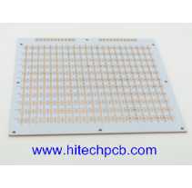
Metal Core PCB
Metal Core PCB, MCPCB Manufacturing Service <br> <br>What is aMetal Core PCB? <br> <br>Metal core aluminum PCB is an aluminum-based copper clad laminate with good heat dissipation function. Generally, the single layer aluminum-based PCB is composed of a three-layer structure, which is a circuit layer (copper foil), an insulating layer and a metal base layer. Also used for high-end use is designed as a double sided and multilayer aluminum PCB. <br> <br>A metal core PCB is a special PCB having a metallic base layer. This base layer is usually made of aluminum or copper. As it contains a metallic layer, it is named Metal Core PCB (MCPCB). <br> <br>An aluminum PCB is a printed circuit board that contains a thin layer of conductive dielectric material. They are also called aluminum cladding, aluminum base, MCPCB (metal clad printed circuit board), IMS (insulated metal substrate), thermal conductive PCB, etc. Aluminum PCBs were developed in the 1970s, and soon their applications increased sharply. The first application is their use in amplifying hybrid integrated circuits. They are being used on a large scale, so we must understand aluminum PCB and its importance. <br> <br>The metallic layer present in the metal core PCB does many wonders along with the dielectric layers. These PCBs are far better than FR-4 PCBs in terms of bearing thermal and pressure stresses. They are suitable for extreme conditions and high heat-dissipating components. Therefore, it has solved many issues that were faced in other PCB substrates. Metal core PCBs have tons of benefits, but all of them come at an additional cost. <br> <br>What is IMS Circuit board ? <br> <br>Insulated Metal Substrate (IMS) <br> <br>The use of IMS circuit boards for simple single-layer circuits is a special but very effective method of heat dissipation for components across circuit boards. These generally consist of aluminium supports, insulation layers and copper foil. The base materials are available in different design versions. <br> <br>Aluminum pcb Applications: <br> <br>LED technology: Illuminated signs, displays and lighting <br> <br>Automotive industry: LED headlights, engine control and power steering <br> <br>Power electronics: DC power supply, inverters and engine control <br> <br>Switches and semi-conductor relays <br> <br>Aluminum pcb Manufacturing process <br> <br>The metal core PCB fabrication process is ①Grinding plate (500# brush)→②Washing→③Passivation→④Washing×3→⑤Blow-drying→⑥Drying. Grinding plate: Grinding the iron surface only, grinding the plate according to FR4 parameters. <br> <br>Metal core PCBs must follow a particular process due to the presence of the metal layer in the stackup. If the board is a single-layer board with no layer transitions back to the metal plate, then the standard FR4 dielectrics can be used, where the dielectric layer is pressed and bonded to the metal plate. <br> <br>For multilayer dielectric stackups, the metal core must first be drilled to allow for a layer transition without creating a short circuit. First, slightly larger holes are drilled into the metal layer, and the holes are plugged with an insulating gel. This gel is cured and hardened, allowing it to be plated with copper, just like a standard via. The rest of the stackup is pressed and bonded with the metal layer, and through-holes are drilled through the stackup, followed by plating and cleaning. <br> <br>The first board must check the circuit without scratches, black tin surface, other defects, and uniform wear marks. <br> <br>Why Choose us for Metal core PCB ? <br> <br>Competitive Cost for PCB Manufacturing <br> <br>We offer high-quality customized PCB Boards with reasonable cost and the best service because we know the cost is significant to a product’s success. We have cost control for each process to provide reasonable PCB costs for our customers. <br> <br>The reason why we can provide you with low-priced PCB manufacturing services is that we have a very complete supply chain management system and maintain a perfect and solid cooperative relationship with suppliers, and through mass procurement and mass production to reduce costs to a greater extent to customers so that you enjoy lower prices than the same industry, higher than the quality of the same industry. <br> <br>Free DFM PCB Design Checking <br> <br>We have a professional engineering team to provide complete engineering support for customers. Free DFM helps to save cost and reduce potential problems during PCB (printed circuit board) manufacturing. <br> <br>Ten professional PCB engineers with over 20 years of PCB experience, with rich experience in various industry standards and process quality requirements, provide customers with optimized design PCB solutions at the design-in stage. <br> <br>Advanced Automatic Production Equipment <br> <br>Advanced PCB manufacturing and PCB assembly Production Equipment, Skilled Technical Workers are the Guarantee of Product Quality. <br> <br>We Guarantee to Provide Reliable Products Based on Advanced Manufacturing Testing Equipments, Well-known Raw Materials and Comprehensive Management Systems. <br> <br>Exquisite PCB Fabrication and PCBA Manufacture Capacity <br> <br>The following is a list of some of our current manufacturing capacity, but not all. In addition, thanks to the fact that we are a private enterprise, in order to meet the needs of customers, we are constantly upgrading our own production equipment and production process. <br> <br>Please trust us. We can provide a one-stop complete service from PCB prototyping to PCB assembly. Please feel free to contact us to find out if we can manufacture your PCB, give us a chance to work with you and give yourself a chance to find a more suitable PCB supplier. <br> <br>Just send us your Gerber file, our professional sales staff will provide you with a fast and accurate PCB quote. <br> <br>[a]https%3A%2F%2Fwww.hitechpcba.com%2Fmetal-core-pcb[/a]
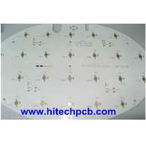
Metal Core PCB
Best Metal Core PCBs By Hitech Circuits! <br> <br>Looking for the best metal core PCBs? Hitech Circuits offers superior aluminum and copper PCB solutions for LED lighting, automotive, telecom, and other demanding applications. With over 10 years of experience, we provide optimized thermal management, increased power density, and maximum durability. <br> <br>As the best metal core PCB manufacturer, our product withstands extreme temperatures to keep components cool even at high power levels. Get the most out of your designs with flexible, high-quality, custom-fabricated metal-core PCBs to your specifications. <br> <br>Trust the metal core PCB experts at Hitech Circuits for unbeatable thermal performance and value. <br> <br>About Our Metal Core PCB <br> <br>Metal core printed circuit boards (PCBs) are vital in applications requiring high heat dissipation. Their enhanced thermal efficiency enables greater power densities while keeping components cool for increased durability. Metal core PCBs also facilitate driving components harder and shaping/forming the circuits. This makes them ideal solutions for the LED lighting industry. <br> <br>Benefits of Using Our PCBs in LED Lighting <br> <br>The lighting sector has evolved tremendously with the help of advanced PCB technologies for superior lumen output. Cost-effective aluminum-backed PCBs in particular, enable the creation of affordable high-performance lighting set-ups. Several advantages make PCBs perfectly suited for LED lighting: <br> <br>Optimized Thermal Management <br> <br>Metal core PCBs like aluminum-backed ones offer the best balance between thermal performance and cost. The metal core enables dissipation of heat more efficiently, increasing component life. <br> <br>Higher Power Densities <br> <br>By keeping components cooler even at higher power inputs, metal core PCBs facilitate greater power densities within smaller hardware footprints. <br> <br>Driving Components Harder <br> <br>The improved cooling capacity provided by metal core PCBs also allows modules and components to be driven at higher operating limits for increased durability and performance. <br> <br>Customizable Shapes <br> <br>Our metal core PCBs can be shaped, drilled, or formed as per application requirements, adding great flexibility. Contact our metal core PCB manufacturer and share your requirements. <br> <br>Structure of Metal Core PCBs <br> <br>Aluminum base copper clad laminate, the raw material for metal core PCBs, has three key layers: <br> <br>Circuit Layer <br> <br>This layer with copper thickness from 1-10oz is equivalent to the copper layer in regular PCB laminates.Dielectric Insulation Layer <br> <br>With a thickness ranging from 0.003” to 0.006”, this special material provides electrical insulation between the circuit and the metal base. It has low thermal resistance for heat transfer and UL certification for safety. <br> <br>Metal Base Layer <br> <br>Usually made of aluminum or copper, this thick metal layer enables heat dissipation from the PCB to the surroundings. <br> <br>Key Characteristics <br> <br>The main characteristics of metal core PCBs are <br> <br>Greatly enhanced thermal management through improved heat spreading and dissipation <br> <br>Optimal balance of thermal performance vs. cost <br> <br>Withstands high temperatures and power levels reliably <br> <br>Types of Metal Core PCBs <br> <br>Some common varieties of metal core PCBs offered are: <br> <br>Single Layer Aluminum Base <br> <br>These PCBs have 3mm aluminum base thickness, 1 oz copper layer, and special thermal dielectric material with thermal conductivity of 3W/mK. <br> <br>Double-Layer Aluminum PCB Boards <br> <br>These allow greater circuit complexity with aluminum thickness from 0.8mm to 3.8mm. Additional coatings like solder or scratch resistance can be applied. <br> <br>Bergquist Brand Metal Core PCB <br> <br>Offering Bergquist aluminum metal core PCB with exceptional 2.4W/mk thermal conductivity for demanding applications. <br> <br>High Current LED Boards <br> <br>Special high thermal conductivity aluminum PCBs designed specifically for high-power LED lighting setups. <br> <br>Customized Metal Core PCBs <br> <br>Fully customized aluminum or copper PCBs fabricated per specific application requirements <br> <br>Call Hitech Circuits For Your Project! <br> <br>As the best metal core PCB manufacturer, we design and develop our products with the ability to handle high power densities. Our metal core PCBs are significant for LED lighting and other heat-generating electronics applications. With various options available, designers now have abundant choices to create efficient and durable systems in compact form factors at optimized costs. <br> <br>Browse our products and call our experts at +86-755-29970700 to make an informed decision. We will gladly help you with your needs. <br> <br>FAQs <br> <br>1. What types of applications use metal-core PCBs? <br> <br>LED lighting, automotive electronics, telecom infrastructure, and other high-power electronics utilize metal-core PCBs for their thermal performance. They are ideal for applications that generate significant heat. <br> <br>2. What metals are used in the base layer of metal core PCBs? <br> <br>Aluminum and copper are the most common base layer metals used. Aluminum provides the best balance of thermal conductivity and cost. Copper offers the highest performance for the most demanding applications. <br> <br>3. What are some key design considerations for metal-core PCBs? <br> <br>Consider the required power levels, operating temperatures, component spacing, board thickness, dielectric material, base metal choice, weight limitations, and special thermal needs. Share your requirements with the PCB manufacturer. <br> <br>4. Can metal core PCBs be customized? <br> <br>Yes, metal core PCBs can be fabricated in different shapes, with various drilling/routing patterns, edge treatments, coatings, and other customizations per specific design needs. <br> <br>5. How can I get started with your metal core PCB fabrication services? <br> <br>Contact our engineering team to discuss your project requirements. We will provide design recommendations, pricing, and manufacturing timelines to deliver high-quality custom metal core PCBs tailored to your application. <br> <br>6. What are the lead times for prototype vs production metal core PCB orders? <br> <br>Prototypes can be delivered in 2-4 days. Production lead times range from 2-4 weeks, depending on order quantity and customization. We can meet urgent delivery needs. <br> <br>[a]https%3A%2F%2Fwww.htmpcb.com%2Fmetal-core-pcb-c-10.html[/a]
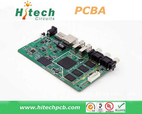
PCB Assembly factory
The pcb assembly factory-Hitech also manufactured printed circuit boards with the highest reliability in all industries. Such as aerospace, defense, automotive, medical and other fields. <br> <br>Technical Parameters <br> <br>We offer a number of services including traditional PCB assembly and Surface Mount (SMT) assembly. Hitechpcb offers turnkey electronic PCB manufacturing services for the medical, industrial control, audio-visual and many other industries with high reliability requirements. Certified to international production standards, our rapid turnaround PCB assembly and comprehensive box build services cover all phases of the production cycle, from design and manufacturing through to distribution.
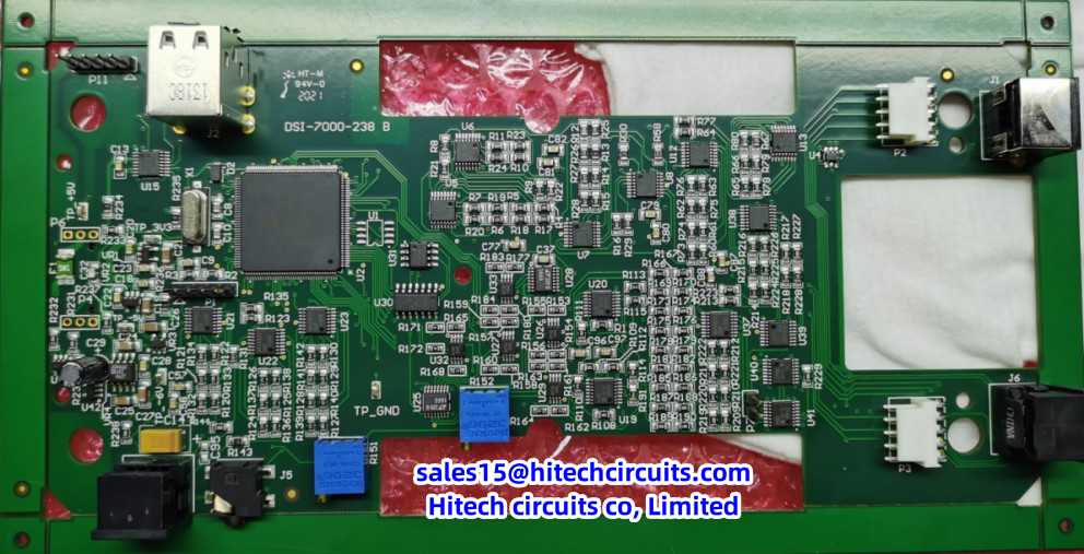
PCB factory
As a leading one-stop electronics manufacturing services provider in China, Hitech Circuits Co., Limited offers high quality, cost effective and quick turn PCB board products, Printed Circuit board, PCB assembly, electronics assembly manufacturing, Electronic parts components sourcing services for your new products development. <br> <br>With mature supply chain, talented design team, advanced manufacturing techniques and quality control systems, Hitech Circuits Co., Limited is able to provide one-stop electronics manufacturing services and solution for our customers to help them stand out in the marketplace. <br> <br>Circuit Board, PCB assembly & electronics manufacturing service provider from China (hitechcircuits.com)
About HDI_PCB Yang's Store
No description provided.
0.0
Customer Reviews
See what others are saying about HDI_PCB Yang's Store. We verify purchases to ensure reviews are genuine.
No reviews yet for this store.