

PCB Assembly's Store
Owned by PCB Assembly Joined Mar 2024 19 Listings
PCB Assembly's Store
easyid.me/biz/pcbassembly-dcbb52 • Verified Store
Scan to open official EasyID digital store, view live catalog, or save business card.
Verified Merchant
EasyID Certified Seller
Fast 24h Packing
Direct courier dispatch
Zero Escrow Direct
Direct merchant settlement
Store Listings (9)
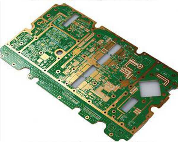
Best High Frequency PCB Manufacturer in China - Hitech Circuits
-Are you dealing with signal transmission or wireless network equipment? One of the key components in these devices is high frequency PCB. <br> <br>These circuits are also important in electronic devices such as mobile phones because they are responsible for data transmission. <br> <br>We introduced these PCBs in detail below, including High -Frequency design, so please continue to read and learn more. <br> <br>-What is a High-Frequency PCB board? <br>Generally speaking, high -frequency high -speed PCB boards refer to printed circuit boards above 1GHz, which may be different in the industry. Its physical performance, accuracy, and technical parameters are very high. They are often used in the fields of communication systems, car ADAS systems, satellite communication systems, and radio systems. But what’s the difference between HDI PCB and normal FR4 PCB. There are high -frequency signal lines on the board or most of the PCB with high -frequency cables as high frequency boards; HDI board refers to a relatively dense line in PCB, mainly such as mobile phones and computer motherboards such as PCB. PCB is now developing in this regard. Ordinary double-sided PCB mainly mean that there are no special types of boards and signals. <br> <br> <br> <br>High frequency (HF) PCB is used to transmit electromagnetic waves at the frequency of GHz. In various applications, the loss in various applications, including mobile, microwave ovens, radio frequency (RF), and high -speed design applications. Therefore, a printing circuit board with certain features is used to transmit these electromagnetic waves. When designing PCB for high-frequency applications, several parameters were considered. <br> <br> <br> <br>When special signal requirements are included in your electronic equipment and products, high-frequency PCB can meet your needs. These higher transmission frequencies can support faster signal flow, which is necessary in today's increasingly complex electronic switches and other components. <br> <br> <br> <br>The increase in the complexity of electronic components and switches continues to require a faster signal flow rate, thereby higher transmission frequency. Because the pulse of electronic components is short, high-frequency technology is also necessary to regard the width of the conductor/track as an electronic component. According to various parameters, high-frequency signals are reflected on the printing circuit board, which means that the impedance must be specified accurately and implemented at the highest process control level.
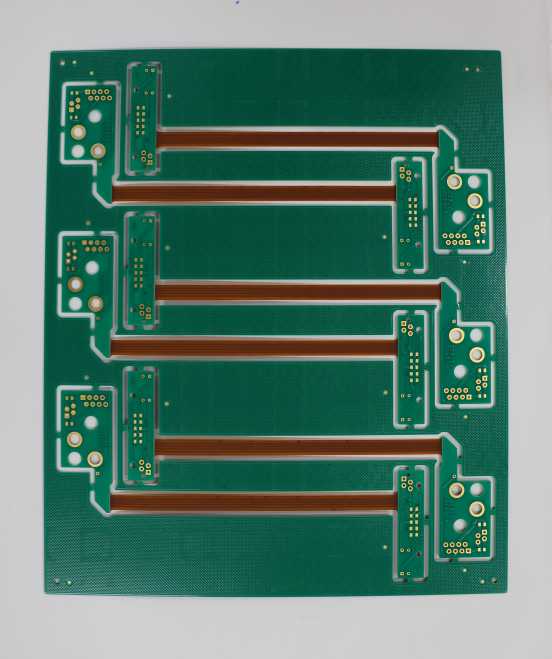
Best Rigid-flex PCB manufacturer up to 18 layers from Hitech Circuits
What are Rigid-Flex Circuit Boards? <br> <br> <br>As the name implies, a Rigid-Flex PCB is a hybrid of a Flex PCB and a Rigid PCB. The combination of the two types of boards utilises the benefits each one provides, integrating the versatility of the flexible board with the robustness of the rigid board. Rigid-flex printed circuit boards are used in more complex mechanical designs, eliminating flexible cables and wiring and replacing it with integrated circuits. <br> <br> <br> <br>Rigid-Flex PCBs, by definition, are a combination of rigid part(s) joined by interconnecting flex areas where the flex material is used across the entire PCB area. <br> <br>The rigid parts are where there is no bending requirement. Again, PTHs take connections from layer to layer as required. Rigid-flex may also employ other technologies as required eg. HDI. Unlike the cost-effective flex PCBs, Rigid-Flex PCBs can be a bit more costly due to their intricate design. <br> <br>Rigid-flex PCB design can be used to eliminate or greatly reduce requirements for bulky and costly cable harnesses, in turn taking out costs and reducing assembly time. Like the pure flexible PCBs, a high volume of rigid-flex PCBs are used in aviation and space applications – and also in automotive and test equipment.
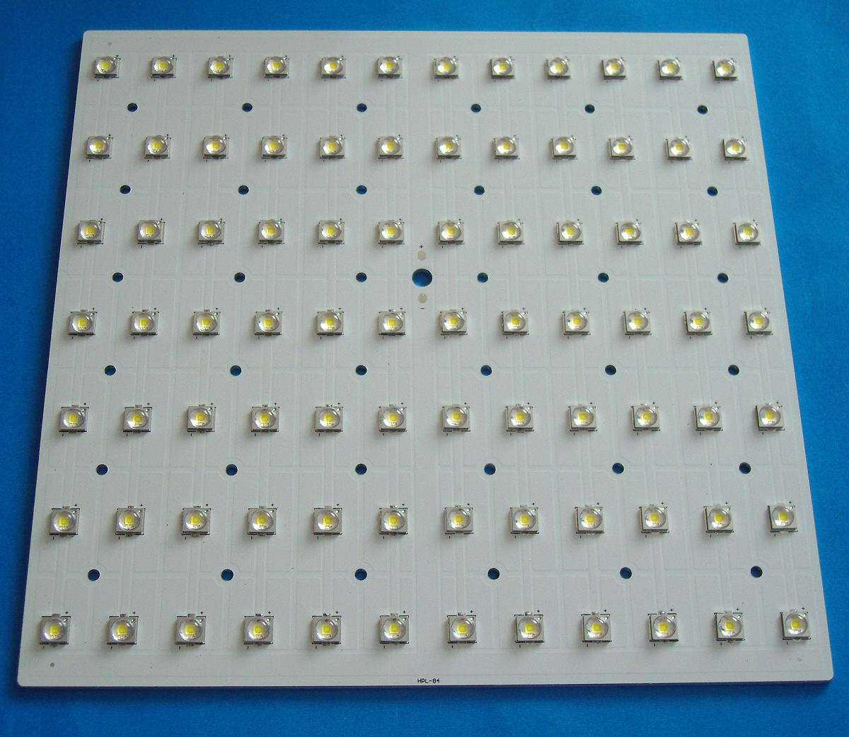
Top 1 LED PCB Board Manufacturing in China
Aluminium LED PCB Board manufacturing <br> <br> <br> <br>Aluminum PCB, or Aluminium PCB, also called Alu PCB, is one of Insulated Metal Substrate (IMS) PCBs, and is also one of the most commonly used Metal Core PCBs (MCPCB) nowadays. HitechPCB manufactures Aluminum printed circuit boards (PCB) with a full selection of high-performance substrates, and we work to be the best aluminum PCB manufacturer and provider no matter you need prototypes or high-volume production quantities. Aluminum PCBs typically are single-sided, but also can be double-sided as well. While, multilayer Aluminum PCBs are highly difficult to manufacture. <br> <br> <br> <br>LED PCB Board <br> <br>Thermal conductivity and thermal resistance of Aluminum LED PCB <br> <br> <br> <br>As a widely used electronic component Aluminum LED PCB's thermal conductivity and thermal resistance are of great significance. The thermal conductivity of led Aluminum LED PCB is the quantity describing the conductor's ability to conduct heat, which can reflect the material's ability to conduct heat. Thermal resistance refers to the change rate of the temperature difference between the two surfaces during the heat conduction process of the surface of the object. In the design and application of electronic components, the thermal conductivity and thermal resistance of led Aluminum LED PCB play a decisive role. <br> <br>Due to the different structure and composition of led Aluminum LED PCB, its thermal conductivity and thermal resistance will be different. Generally speaking, the greater the thermal conductivity of the led Aluminum LED PCB, the stronger the heat conductivity of the surface; And the smaller the thermal resistance, the smaller the temperature difference between the two surfaces. To sum up, the thermal conductivity and thermal resistance of led Aluminum LED PCB are very important parameters, which can affect the performance and service life of electronic components. <br> <br>For different application requirements, the thermal conductivity and thermal resistance of led Aluminum LED PCB will be different. For example, in high temperature environments, Aluminum LED PCB with low thermal resistance and high thermal conductivity should be used; On the contrary, if it is in a low temperature environment, the Aluminum LED PCB with large thermal resistance and small thermal conductivity should be selected. Therefore, in the process of design and application, the thermal conductivity and thermal resistance of Aluminum LED PCB should be selected scientifically and reasonably according to the actual use environment and demand, so as to obtain better use effect. Hitech can provide a wide range of aluminum-based LED PCBS to suit customer requirements. <br> <br> <br> <br>The relationship between insulating layer thickness and pressure resistance of Aluminum LED PCB <br> <br> <br> <br>Aluminum LED PCB is a kind of basic material widely used in the field of electronics. The selection and thickness of insulating layer must be considered in the production process. Insulation layer is an important part of Aluminum LED PCB, its role is to prevent short circuit and leakage between different components on the circuit board, so as to ensure the normal operation of the entire circuit. The thickness of insulation layer is very important to the performance of Aluminum LED PCB and is closely related to the voltage it can withstand. <br> <br>In general, the thicker the insulating layer of Aluminum LED PCB, the higher the voltage it can withstand. Because the thicker the insulation, the better you can isolate the different components on the board, reducing the possibility of short circuits and leakage. In addition, the thickness of the insulation layer can also affect the durability and stability of the Aluminum LED PCB, making it more durable and reliable. <br> <br>However, too thick insulation can also bring unnecessary costs and manufacturing difficulties. Therefore, factors such as cost, reliability and performance must be considered comprehensively when selecting insulation layer thickness. Generally, the insulating layer thickness of Aluminum LED PCB should be between 5mil and 10mil, but can be adjusted for specific application requirements. For higher voltage requirements, a thicker insulation layer should be selected to ensure the stability and safety of the circuit board. <br> <br>In summary, the insulating layer thickness of Aluminum LED PCB is closely related to its pressure resistance. Choosing the appropriate insulating layer thickness can improve the safety, stability and reliability of Aluminum LED PCB, so as to ensure the normal operation of the entire circuit. However, in the process of production, it is necessary to consider cost and performance factors to choose the most appropriate insulation layer thickness. <br> <br> <br> <br>Aluminium LED PCB <br> <br>Thermal expansion of Aluminum LED PCB <br> <br> <br> <br>Aluminum LED PCB is a unique metal substrate covered with copper substrate, it has good thermal conductivity, heat dissipation, electrical insulation and mechanical properties. Now let's talk about some properties of Aluminum LED PCB: <br> <br>a. Thermal expansion of Aluminum LED PCB: <br> <br>Thermal expansion and cold contraction is the common nature of substances, and the thermal expansion coefficient of different substances is different. Aluminum LED PCB can effectively solve the problem of heat dissipation, so as to alleviate the problem of thermal expansion and cold contraction of components on PCB board, and improve the durability and reliability of the whole machine and electronic equipment. In particular, the problem of hot expansion and cold contraction of SMT technology is solved. <br> <br>b, heat dissipation: <br> <br>At present, for many PCB boards with high density and power of double panels and multilayer boards, heat emission has become the most common difficulty. For example, FR4 and CEM3 are bad conductors of heat, interlayer insulation, and heat emission cannot go out. Local heating of electronic equipment cannot be excluded, leading to high temperature failure of electronic components. Thus it is widely used in high-power electronics, automobile electronic control, new energy savings, 5G communication products. <br> <br>c, the ruler of Aluminum LED PCB is relatively stable, obviously the size is much more stable than that of the printed board of insulating materials. Aluminum LED PCB and aluminum sandwich board, from 30 degrees Celsius to 140~150 degrees Celsius C heating, the size change is 2.5~3.0%. <br> <br>d, with shielding effect, instead of brittle ceramic substrate, safe use of surface mounting technology, reduce the real effective area of PCB board, replace the radiator and other components, improve the heat resistance and physical properties of the product; Reduce production costs and labor costs, <br> <br>e. Structure: 1) a. aluminum base material, the use of LF, L4M, Ly12 aluminum, the expansion strength of 30kaf/mm2, elongation of 5%. Aluminum substrate is divided into 1.01.6, 2.0, 3.2mm 4 kinds, Aluminum models 6061T6 or 5052H34• Panasonic Electric, Sumitomo R-0710, R-0771, AL C-1401ALC-1370 and other models are aluminum base copper clad plate, the current thickness of aluminum base is 1.0~6.0mm. 2) insulation, usually 50~200um• If too thick, Can play the role of insulation, prevent and metal base short circuit effect is good, but will affect the heat dissipation if too thin, can be good heat dissipation, but easy to cause the metal core and component lead short circuit • Insulation layer (or semi-cured sheet), placed on the anodized, insulated aluminum plate, after laminating with the surface of the copper layer firmly combined together <br> <br>Aluminum plate in the production of: <br> <br>(1) aluminum oxide processing: strong oil cleaning (hydroxide) -- -- dilute acid neutralization, coarsening (aluminum plate surface to form honeycomb) -- -- oxidation (um) -- - alkali neutralization -- -- the bore is sealed by baking. Each process must ensure the quality or affect the adhesion of Aluminum LED PCB. <br> <br>(2) The entire production process is not allowed to wipe the aluminum base surface, can not touch the aluminum base, damp and other dye, otherwise affect the Aluminum LED PCB bonding on it. Hitech in the production process strictly control each process, to provide customers with high quality Aluminum LED PCB. <br> <br> <br> <br>Types of Aluminum LED PCB <br> <br> <br> <br>Aluminum base plate commonly used metal aluminum base plate mainly 1000 series, 5000 series, 6000 series. The basic characteristics of these three series of aluminum are as follows: <br> <br>(1) 1000 series on behalf of 1050, 1060, 1070, 1000 series aluminum plating, also known as pure aluminum plate. Of all series, Series 1000 contains the most is 2 layers of Aluminum LED PCB, purity can reach more than 99.00%. Because it does not contain other technical elements, the production process is relatively simple and the price is also relatively cheap. It is the most commonly used series in traditional industries. Most of the products in circulation are the 1050 and 1060 series. <br> <br>The 1000 series aluminum plate is based on the last two digits to determine the minimum aluminum content of the series. For example, the last two digits of 1050 series are 50. According to the international brand naming principle, its aluminum content must reach 99.5% or more to be qualified. In the country's aluminum alloy technical standard (GB/T3880-2006), it is also clearly stipulated that the aluminum content of 1050 should reach 99.5%. Similarly, the 1060 series aluminum plate must contain more than 99.6 percent aluminum. <br> <br>(2) 5000 series stands for 5052, 5005, 5083 and 5A05 series. 5000 series aluminum plate belongs to the more commonly used alloy aluminum plate series, the main element is magnesium, magnesium content between 3-5%, also known as aluminum magnesium alloy. It is characterized by low density, high tensile strength and high elongation. In the same area, the weight of aluminum magnesium alloy is lower than other series, <br> <br>So it is often used in aviation, such as aircraft fuel tanks. In addition, it has a wide range of applications in traditional industries. Its processing technology is continuous casting and rolling, belonging to the hot rolled aluminum plate series, so it can be used for oxidation deep processing. In our country, 5000 series aluminum plate is one of more mature aluminum plate series. <br> <br>(3) 6000 series represents 6061, mainly containing magnesium and silicon, so the advantages of 4000 series and 5000 series are concentrated. 6061 is a cold treatment aluminum forgings, suitable for corrosion resistance, oxidation resistance requirements of the occasion. It has good mach inability, excellent interface characteristics, easy coating, good processing performance. <br> <br>General characteristics of 6061: excellent interface characteristics, easy coating, high strength, good workability, strong corrosion resistance. Typical uses of 6061 aluminum: aircraft parts, camera parts, couplers, Marine parts and hardware, electronic parts and connectors, etc. <br> <br>Comprehensive consideration of the material itself texture, hardness, elongation, chemical properties, price and other factors, Aluminum LED PCB generally used 5000 series aluminum alloy 5052 aluminum plate. <br> <br> <br> <br>LED PCB Board manufacturing <br> <br>Surface treatment technology of Aluminum LED PCB <br> <br> <br> <br>After the electrical parts are inserted into the printed circuit board, they should be welded automatically. In these processes, if the material bubbling, in addition to the printed circuit board processing technology is not reasonable, but also related to the Aluminum LED PCB dip welding resistance. The poor impregnation and weld ability of Aluminum LED PCB will lead to the reduction of system quality stability and the damage of the whole components. Therefore, Aluminum LED PCB manufacturers attach great importance to the quality problem of impregnation and weld ability, which directly affects the product reputation of each manufacturer. <br> <br>Aluminum LED PCB is a composite of resin, aluminum and copper foil curing. The thermal expansion coefficient of resin and aluminum, copper foil is very different, therefore, under the action of external force and heat, the internal force distribution of the plate is not uniform. If there are water molecules and some low molecules in the pores of the plate interface, under the condition of thermal shock, it will produce greater concentrated stress. If the adhesion can not resist these internal destructive forces, it will occur on the weak interface of copper foil and substrate, or lamination and foaming between the substrate layers. <br> <br>To improve the weld resistance of Aluminum LED PCB, it is necessary to reduce the factors that will destroy the structure of various surfaces in the forming and high temperature of the plate. The improvement methods mainly include the surface treatment of copper foil and aluminum, the improvement of resin adhesive, and the control of pressure and temperature in the pressing process. Hitech circuits mainly on Aluminum LED PCB aluminum surface treatment to do some expressions. <br> <br> <br> <br>Properties of aluminium substrates and surface treatment of materials <br> <br> <br> <br>Aluminum LED PCB, is a kind of raw material, is a kind of metal base copper plate with good heat dissipation function. It is an electronic glass fiber cloth or other reinforcing materials soaked in resin, a single resin as insulating bonding layer, one or two sides covered with copper foil and made of hot pressing and made of a plate material, known as copper clad laminate Aluminum LED PCB, referred to as aluminum clad copper plate. <br> <br>(1) Excellent heat dissipation performance <br> <br>Aluminum clad copper foil plate has excellent heat dissipation performance, which is the most outstanding characteristic of this kind of plate. The PCB made from it can not only effectively prevent the working temperature rise of the components and substrate loaded on it, but also rapidly dissipate the heat generated by the power amplifier components, high-power components, large circuit power switches and other components. In addition, because of its low density and light weight (2.7g/cm³), it can prevent oxidation and has a low price. Therefore, it has become the most widely used composite plate. The saturated thermal resistance of the insulated Aluminum LED PCB is 1.10℃/W and 2.8℃/W, which greatly improves the fusing current of the copper wire. <br> <br>(2) Improve the efficiency and quality of machining <br> <br>Aluminum clad copper plate has high mechanical strength and toughness, which is much better than rigid resin clad copper plate and ceramic substrate. It can realize the manufacture of large area printed boards on metal substrates, especially suitable for mounting heavy components on such substrates. In addition, the Aluminum LED PCB also has good flatness, which can be used for hammering, riveting and other aspects of assembly processing on the substrate or bending and twisting along the non-wiring part of the PCB made of it, while the traditional resin copper clad plate can not. <br> <br>(3) High stability of size <br> <br>There is a problem of thermal expansion (dimensional stability) for all kinds of copper clad plates, especially the thermal expansion in the thickness direction of the plate (Z axis), so that the quality of metallized holes and lines is affected. The main reason is that the linear expansion coefficient of the plate is different, such as copper, and the linear expansion coefficient of epoxy glass fiber cloth substrate is 3. The linear expansion of the two is very different, easy to cause the thermal expansion of the substrate difference, resulting in copper wire and metallized hole fracture or damage. The linear expansion coefficient of the Aluminum LED PCB is between, it is much smaller than the general resin substrate, and more close to the copper linear expansion coefficient, which is conducive to ensure the quality and reliability of the printed circuit.
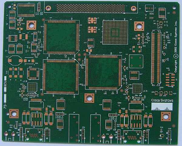
Multilayer PCB Manufacturing up to 38 Layers
Multilayer PCB Manufacturing up to 38 Layers <br>Multilayer PCB Manufacturing up to 38 layers <br> <br> <br> <br>Rigid Circuit Board Manufacturer & Assembly – One stop service PCB rigid Circuit Board is an important electronic component, support for electronic components, and a carrier for electrical connection of electronic components. Read on to learn more about multilayer PCBs, their uses and advantages in the world of modern electronics. <br> <br> <br> <br>A Multilayer Printed Circuit Board, or Multilayer PCB, is a complex circuit board composed of multiple layers of conductive material and insulating material (usually fiberglass and epoxy resin) sandwiched together. Multilayer PCB or multilayer printed circuit boards are circuit boards composed of two or more conductive layers (copper layers). The copper layer is pressed together by the resin layer (prepreg). Each layer has a conductive path or copper trace, and each layer is connected to one another through pads and vias, which act as electrical conduits. This construction allows for more complex and dense circuitry to be designed, with greater functionality and reliability compared to single- or double-sided PCBs. Multilayer PCBs are commonly used in electronic devices such as computers, smartphones, and advanced medical equipment. <br> <br> <br> <br>Multilayer PCB Prototype manufacturing <br> <br>What is Multilayer Printed Circuit Board? <br> <br> <br> <br>A Multilayer Printed Circuit Board (PCB) is a type of PCB that consists of several layers of conductive material and insulating material sandwiched together. The board is made by laminating together multiple thin layers of fiberglass or other insulating materials with copper foil. <br> <br>An integrated circuit is placed on the board, and the copper traces connected to the circuit are etched onto the inner layers of the board. The inner layers are then sandwiched together with the outer layers, forming a multilayer structure. <br> <br>Multilayer PCBs are used in high-end electronic products, such as advanced computers and mobile phones, where a high degree of density is required, and the manufacturing process is complex. They provide many benefits, including reduced size, increased reliability, and improved performance. <br> <br>Multilayer PCBs are cost-effective because they reduce the total number of components needed and improve product reliability, thus reducing the need for frequent repair services or replacement. The design flexibility of these boards also allows for more efficient use of space and improved signal routing, which aids in the performance of the product. <br> <br> <br> <br>Multilayer Printed Circuit Board stack up <br> <br> <br> <br>So what’s Multilayer PCB Benefits / Advantages? <br> <br> <br> <br>1. Increased Design Flexibility: Multilayer PCBs allow for more design flexibility and greater circuit density. With multiple layers, engineers have more space to incorporate more components and features, such as impedance control, shielding, and power planes, within the same board area. <br> <br> <br> <br>2. Increased Reliability: Multilayer PCBs are more reliable than single sided PCBs, as they are less prone to issues such as signal interference, voltage drops, and thermal stress. This is because they have a higher number of conductive layers, which allows for better shielding and more stable power distribution. <br> <br> <br> <br>3. Higher Component Density: Multilayer PCBs can accommodate a higher density of components in a smaller space while preventing signal interference. This results in a more compact and efficient design, saving manufacturers money on materials and production. <br> <br> <br> <br>4. Improved Signal Integrity: With a multilayer construction, PCBs can have better signal integrity, which means less noise and less chance of signal interference. The numerous grounds and power planes help to suppress electromagnetic interference, resulting in better connection quality. <br> <br> <br> <br>5. Better Thermal Management: Multilayer PCBs have better thermal conductivity, which reduces hot spots and improves heat dissipation. The extra layers also help to keep the heat from spreading across the board, which is important for high-power applications. <br> <br> <br> <br>6. Cost-Effective: While the initial cost of multilayer PCBs may be higher than single or double-sided PCBs, the benefits in terms of increased density, reliability, and design flexibility can mean overall cost savings in the long run. Additionally, as manufacturing techniques have evolved, the cost of producing multilayer PCBs has become more competitive. <br> <br> <br> <br>In summary, the benefits of multilayer PCBs include increased design flexibility, reliability, component density, and thermal management. They also offer improved signal integrity and can be cost-effective in the long run. These advantages make them suitable for complex electronic devices where high performance, reliability, and space-saving are required. <br> <br> <br> <br> <br> <br>-While Multilayer Printed Circuit Boards (PCBs) offer many benefits over single- or double sided PCBs, there are also some potential drawbacks to consider: <br> <br> <br> <br>1. Complexity: The multilayer PCBs are far more complex than their single-layered or double-layered counterparts. As the number of layers increases, so does complexity. This means that design and manufacturing is more challenging, which can lead to a higher cost of production. <br> <br> <br> <br>2. Cost: Multilayer PCBs are generally more expensive than single or double-layered PCBs due to their complexity. The cost of producing multilayer PCBs can increase exponentially, and the cost of manufacturing is highly dependent on the number of layers in the board, the board size, and overall complexity. <br> <br> <br> <br>3. Signal Integrity: Multilayer boards pose a higher risk of signal integrity issues due to the higher number of components and traces present in each layer. Signal interference, crosstalk, and noise can occur if proper precautions are not taken in the design process. It is therefore essential that the designer takes signal integrity into account while designing the board. <br> <br> <br> <br>4. Manufacturing Challenges: The process of cutting, etching, drilling, and laminating the multiple layers of a PCB requires highly precise equipment, which can add to the cost of manufacturing. Moreover, misalignment of layers and flaw in lamination can lead to defects that can potentially cause the PCB to stop functioning correctly. <br> <br> <br> <br>5. Environmental Impact: Multilayer PCBs contribute to electronic waste, which is a significant concern for the environment. The process of manufacturing multilayer PCBs consumes a considerable amount of energy, and the resulting waste can be toxic and difficult to recycle. <br> <br> <br> <br>Overall, Multilayer PCBs offer many advantages over single or double-sided PCBs. However, there are several issues that need to be considered during the design and manufacturing process, to achieve optimal performance. To solve your problems, here HITECH Circuits provide solutions for you. <br> <br> <br> <br>Multilayer Printed Circuit Board <br> <br> <br> <br>-Multilayer Printed Circuit Boards (PCBs) are used in a variety of applications where high performance and reliability are critical. Here are a few of the most common applications: <br> <br> <br> <br>1. Communications: Multilayer PCBs are widely used in the telecommunications industry for various applications such as cell phone base stations, satellite communications systems, and other communication devices that require high-speed data transfer rates and minimal signal loss. <br> <br> <br> <br>2. Computers: Multilayer PCBs are extensively used in computer motherboards, laptops, and other computing systems where high performance, reliability, and miniaturization are of utmost importance. <br> <br> <br> <br>3. Medical Equipment: Multilayer PCBs are a key component in many medical devices, such as imaging equipment, patient monitoring systems, and surgical instruments, where high reliability and stability are required. <br> <br> <br> <br>4. Automotive: The automotive industry uses Multilayer PCBs for applications such as engine control units, airbag systems, and lighting control systems, where reliability, durability, and efficient operation are essential. <br> <br> <br> <br>5. Aerospace and Defense: Multilayer PCBs find extensive use in aerospace and defense applications, such as missiles, satellites, and other spacecraft, where superior performance and reliability are required in extreme conditions. <br> <br> <br> <br>Overall, Multilayer PCBs are used in a wide variety of applications where increased functionality, reliability, and performance are required. With advances in technology, the use of multilayer PCBs is expected to continue to grow in the future.
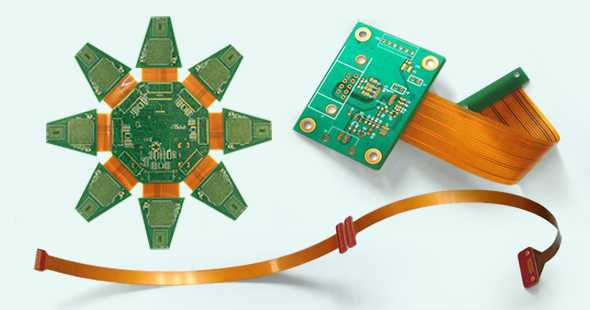
Best Flexible PCB Manufacturing
What is Flex PCB? <br> <br> <br> <br>Flexible printed circuits, also known as flex circuits, are sometimes regarded as a printed circuit board (PCB) that can bend, when in reality there are significant differences between PCB’s and flex circuits when it comes to design, fabrication and functionality. One common mistake that designers make is to design a flexible circuit using the same rules as a PCB. Flex PCB require a unique set-up and have their own set of design rules that the Hitechpcb team has termed “flex-izing” and have worked hard to perfect over the last many years. <br> <br> <br> <br>Flexible PCB, which also called Flex PCB, Flexible circuit board or flex circuit, it consists of PI base material, adhesive layer, copper layer, coverlay and sometimes with stiffeners. Flexible PCBs are now being used widely to replace traditional FR4 PCB in various different applications due to the benefits from flex PCB specially. Although more expensive than a normal rigid PCB, the right design in the right application could save weight and time in assembly, coupled with the reliability which makes flexible circuit board a worthwhile consideration. <br> <br> <br> <br>A flexible printed circuit consists of a metallic layer of traces, usually copper, bonded to a dielectric layer, usually polyimide. Thickness of the metal layer can be very thin (<.0001″) to very thick (> .010″) and the dielectric thickness can vary from .0005″ to .010″. Often an adhesive is used to bond the metal to the substrate, but other types of bonding such as vapor deposition can be used to attach the metal. <br> <br> <br> <br>flexible PCB <br> <br>How to calculate your flex pcb bend radius? <br> <br> <br> <br>Because copper tends to readily oxidize, the exposed surfaces are often covered with a protective layer, gold or solder are the two most common materials because of their conductivity and environmental durability. For non-contact areas a dielectric material is used to protect the circuitry from oxidation or electrical shorting. <br> <br> <br> <br>The number of material combinations that could go into a flexible printed circuit are nearly endless; current, capacitance, chemical and mechanical resistance, temperature extremes and type of flexing are just some of the criteria that impacts the material selections that best meet the functional needs. An experienced Hitechpcb design engineer takes the critical requirements into consideration when designing a circuit to meet your needs. <br> <br> <br> <br>Flexible printed circuit boards (FPC) has become a common component of electronic products due to its lightness and flexibility performance. It is widely used in smart terminal, wearable electronics, consumer, automotive, industrial and medical fields. The miniaturization and integrated function of electronics product development is driving FPC to fine line and multilayer design. <br> <br> <br> <br>What is Multilayer flex PCB? <br> <br>This type of flexible printed wiring boards are multilayered (with three or more conductor layers) and require plated-through holes. We could use through vias, buried vias and blind vias. <br> <br> <br> <br>A multi layer flex circuit combine several single-sided or double-sided circuits with complex interconnections, shielding and/or surface mounted technologies in a multi layer design. The multi layers may or may not be continuously laminated together throughout the production process. If your design needs require maximum flexibility, continuous lamination may not be appropriate. Multi layer circuits are an effective solution when confronted with design challenges such as: unavoidable crossovers, specific impedance requirements, elimination of crosstalk, additional shielding and high component density. You can also link here to learn more about flex pcb bending radius. <br> <br> <br> <br>Benefits to Flex PCB including: <br> <br>Assembly Error Reduction <br> <br>Decreased Assembly Time and Costs <br> <br>Design Freedom <br> <br>Flexibility during Installation <br> <br>High Density Applications <br> <br>Improved Airflow <br> <br>Increased Heat Dissipation <br> <br>Increased System Reliability <br> <br>Point-to-Point Wire Replacement <br> <br>Reliability and Durability <br> <br>Repeatable Routings <br> <br>Simplified Circuit Geometry <br> <br>Package Size and Weight Reduction <br> <br>Flex PCB Static Application <br> <br>An application where flexible circuits are flexed only to install the circuit and fit it into its application (also known as flex-to-fit or flex-to-install). A static application will typically be made using the less expensive Electro Deposited (ED) copper. <br> <br> <br> <br> <br> <br>Flex PCB Dynamic Flexing Applications <br> <br>A situation where the flexible circuit itself is dynamically (repeatedly) flexed during the actual use of the final product. Common examples include flip-type cell phones, laptops, printer heads and robotic arms. A dynamic application will require the use of Rolled Annealed (RA) copper. <br> <br> <br> <br>High Density Flex PCB Applications <br> <br>Flexible circuits allow for minutely narrow lines giving way to high density device population. Denser device populations and lighter conductors can be designed into a product, freeing space for additional product features. <br> <br> <br> <br>With a large number of investments on the facilities of flexible printed circuit board and continuously innovating the flexible circuit board manufacturing technology, Hitech Circuits is able to manufacture flexible PCBs with a great variety of technologies, from simple single sided flex PCB, double sided flex PCB to complex multilayer flexible PCB, Rigid flex pcb and support prototype FPC with laser cutting & flying probe test to mass production with toolings. <br> <br> <br> <br>Multilayer flex PCB bookbinding <br> <br>Circuit bookbinding is one of the best practices employed by Hitechpcb engineers for creating stacked PCBs. For flex PCBs, we offered a 12 layer flex PCB board with bookbinding. An additional small length is added to the circuit, making it move in an outward direction from the bend radius. There are copper traces placed at right angles to the bend. This helps restrict the circuit bend in one direction. <br> <br> <br> <br>The length to be added depends on total number of layers in the PCB, as well as the tightness of the bend. The advantage of circuit bookbinding is that it removes a great amount of tension from the various circuit layers during the bending process. The method also helps prevent buckling of the circuits at the exact bend radius. <br> <br> <br> <br>The bookbinded PCBs can easily meet the tight tolerance requirements in comparison to bonded PCBs. This is why this 12 layer flex PCB is a perfect choice for applications where stricter tolerances are required. Its polyamide construction delivers immense strength and flexibility. This flexi PCB can easily perform 180° bends. Also, the construction helps prevent buckling of inner layers, which often occurs in a long term use. This flexibility also helps reduce stress on the internal components. This 12 layer flex PCB board has better shelf life than a 12 layer bonded circuit board. The immersion gold plating offers low contact resistance, good wetting, as well as excellent shelf life. We can provide the 12 layer flex PCB board with book binding in width 4/4 mil, with minimum finish thickness 0.15 mm flex and maximum 1.6 mm. <br> <br> <br> <br>Advantages of Flexible PCB <br> <br> <br> <br>Flexible PCB technology often has a wide range of possibilities for different designs and products. <br> <br>The flexible feature is among the best attributes of the cables, wires, connectors and even PCBs. <br> <br>Some of the advantages of using the flexible circuit include: <br> <br> <br> <br>Reduces the overall weight and size. <br> <br>A flex circuit can reduce the weight of a device by up to 70%. <br> <br>Improves the packaging of electronics <br> <br>It gives you the ability to solve interconnect and packaging issues as it can bend, form and move. <br> <br>Interconnect solution as it reduces the amount of interconnects such as cables, wires, pcbs and connectors. <br> <br>Conformability as the slender nature of the material allows for making of 3D packages <br> <br>Electrical integration – You can easily come up with custom solutions basing your design on a plethora of choices of materials. Apart from that, you have the freedom to choose from the myriad of designs and plating procedures. <br> <br>Heat dissipation ability or power – The polyimide dielectric has the ability to withstand very high temperatures. You can, therefore, use it for high power applications. <br> <br>Electrical and mechanical repeatability <br> <br>Cost saving as you can save up to 30% of the total cost of hand wiring and other assembly processes. <br> <br>You can also save on space by almost 30% <br> <br>It is more reliable as it does not have any wiring errors <br> <br>Despite the numerous advantages, the flexible PCB also has its disadvantages. <br> <br>Let’s have a look. <br> <br> <br> <br>Disadvantages of Flexible PCB <br> <br>Every electronic solution must have certain demerits. <br> <br>Some of the disadvantages include: <br> <br>Flexible PCB <br> <br>A higher initial cost – Since the flex circuit is often custom for particular electronics. The initial cost of designing, photographic plate and layout is very high. This limits you to using it on large quantities to save on cost. <br> <br>Flexible circuit repairs and changes are very difficult – The initial process is not just expensive but difficult to come up with. Once you have the base map, it becomes difficult to make any more changes. Removing and replacing the covering film for repair is also extremely difficult. <br> <br>It is often small in size – The batch process of making the flexible circuits often limits the size of the flexible circuit. The production equipment limits you from making wider and longer sizes. <br> <br>Easy to damage – Improper personal operations can easily damage the flexible circuits. Rework and soldering will require the expertise of a technician. <br> <br>The process of assembly is also very difficult. <br> <br>Do not let the disadvantages kill your spirits. <br> <br> <br> <br>Why Not Make All Circuit Boards Flexible? <br> <br> <br> <br>Flexible circuit boards are certainly useful, but they are not going to replace rigid circuit boards for all applications. Cost efficiency is the main obstacle to implementing an exclusively flexible circuit board design in a consumer product. Rigid circuit boards are less expensive to manufacture and install in a typical automated high-volume fabricating facility. <br> <br> <br> <br>Typically, the ideal solution for an innovative product is one that incorporates flexible circuitry when necessary and employs solid, reliable rigid circuit boards where possible to keep manufacturing and assembly costs down. <br> <br> <br> <br>Some manufacturers even use hybrid rigid-flex printed circuit boards expressly for this purpose. This is common in laptop computers and medical devices, where rigid circuit boards can be connected to one other using ribbon-like flexible circuits. These boards can be compounded and designed to meet any number of engineering needs by focusing on the respective strengths of each circuit board base technology. <br> <br> <br> <br>Hitech Circuits creates both flexible and printed circuit boards for product manufacturers. Enjoy a consultation with one of our sales reps to find out if your product prototype design is best served by flexible or rigid circuit board types. <br> <br> <br> <br>What is Flexible PCB and Its Production Process? <br> <br> <br> <br>Flexible PCB (Flexible Printed Circuit, FPC) is very popular with excellent characteristics such as low weight and thin thickness, etc. It is also can be folded freely. Flexible PCB mainly relies on manual visual inspection with high cost and low efficiency. With the rapid development of the electronics industry, the design of printed circuit board has become more and more high -precision and high- density, traditional manual testing methods can no longer meet production needs. FPC defect automation testing has become an inevitable trend of industrial development. <br> <br>Flexible printed circuit (FPC) is a technology developed by theUnited Statesto develop aerospace rocket technology in the 1970s. It is high reliability, excellent deflection made by polyester film or polyimide as a substrate material. A flexible circuit is formed by embedding a circuit design in a thin, flexible plastic sheet that is flexible, allowing a large number of precision components to be stacked in a narrow and limited space. This circuit can be bent and folded at will. Flexible has the characteristics like light weight, small size, good heat dissipation, easy installation, etc, it breaks through the traditional interconnection technology in the structure of the flexible circuit, the material is composed of insulating film conductor and adhesive <br> <br> <br> <br>Flexible PCB includes single sided FPC, double sided FPC and multilayer FPC, etc. Single FPC has chemically etched conductive pattern layer, the conductive pattern layer on the surface of the flexible insulating substrate is calendered copper foil. The insulating substrate may be polyimide, polyethylene terephthalate, arylamide fiber ester and polyvinyl chloride. The double sided FPC on both sides of the insulating base has a conductive graphics made of etching, which increases the wiring density of the unit area. Metal hole connects the graphic connection on both sides of the insulation material to form a conductive pathway to meet the flexible design and function. The covering film can protect the single, double -sided wire and indicate the position of the component placed. According to demand, metal holes and coverage layers are optional. This type of Flexible PCB has fewer applications. Multi -layer flexible PCB is to press the single-sided or double-sided flexible circuit layer of 3 or more layers together. The metal hole is formed by drilling and electroplating, and conductive channels are formed among different layers. In this way, there is no need to use a complex welding process. Multi-layer circuits have huge functional differences in higher reliability, better thermal conductivity and more convenient assembly performance. <br> <br> <br> <br>At present, the production process of flexible PCB mainly includes looping, Sizing conductor, etching, routing of the conductors, ground planes, sizing of the holes, filleting, button plating, adhesive-backed films, screen-print liquid overcoats, photo imaginable liquid, film polymers and other processes. See the figure for the specific production process.
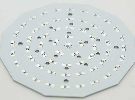
Aluminum PCB & Metal Core PCB & LED PCB Circuit board
Aluminium PCB are metal-based, copper-clad laminates with a good heat dissipation function. Usually, Aluminium PCB is refer to LED PCB board, which is the most important part of LED display and lighting products, etc. <br> <br>Hitech Circuits Co., Limited is a professional aluminum pcb board, LED PCB manufacturer in China. Through 10 years of aluminum pcb board designing and manufacturing experience, Hitech are able to provide high quality and cost effective single layer, double layer and multi layer aluminum pcb boards to global customers. For any of your requirements regarding aluminum pcb board, please don’t hesitate to contact [email protected] . <br> <br>What is aluminium PCB board ? <br>Aluminium PCB board, also named Aluminium based PCB, metal clad (MCPCB) PCB, insulated metal substrate(IMS or IMPCB) PCB, thermally conductive PCBs, etc. Aluminum printed circuit board ( PCB ) is a unique metal-based copper clad laminate with good thermal conductivity, electrical insulation performance and mechanical processing performance. It is composed of copper foil, thermally conductive insulating layer and metal substrate. It is generally including single layer, double layer and multi layer aluminum pcb board. <br> <br>The structure of aluminum printed circuit boards <br>Generally speaking, the PCB aluminum substrate is composed of a circuit layer, a thermally conductive insulating layer and a metal base layer; it can be divided into three layers: <br> <br>Circuit layer: equivalent to the copper clad laminate of an ordinary PCB, the thickness of the circuit copper foil is 1 to 10 oz. The circuit layer (that is, copper foil) is usually etched to form a printed circuit to connect the various components of the assembly. Generally, the circuit layer requires a large current-carrying capacity, so thicker copper foil should be used, with a thickness of 35μm~ 280μm; <br> <br>Insulation layer: The insulation layer is a layer of low thermal resistance thermally conductive insulating material. The thickness is 0.003 to 0.006 inches. It is generally composed of a special polymer filled with special ceramics. It has low thermal resistance, excellent viscoelasticity, thermal aging resistance, and can withstand mechanical and thermal stress. It is the core technology of aluminum-based copper clad laminates. Our aluminum printed circuit boards have obtained UL certification. <br> <br>Metal base layer: The metal base layer is the support member of the aluminium pcb, which requires high thermal conductivity, generally aluminum plate will be used, copper plate can also be used (copper plate can provide better thermal conductivity), suitable for conventional machinery such as drilling, punching and cutting processing. <br> <br>Main usages and applications of aluminium PCB board: <br>Audio devices: input, output amplifiers, balanced amplifiers, audio amplifier, preamplifier, power amplifier etc. <br>Power Supply: switching regulator, DC / AC converter, SW regulator . <br>Telecommunications electronic equipment: high-frequency electric amplifiers, filtering appliance, transmitter circuit etc . <br>Office automation equipment: electric motor, drivers etc . <br>Automotive: electronic regulator, ignition, power controllers etc . <br>Computer: CPU board, floppy drive, power device etc . <br>Power Modules: converter, solid-state relay, power rectifier bridges etc . <br>Lamps Lighting: with the promotion of energy-saving lamps, Aluminum base PCB , are widely used on LED lights. <br>Aluminum pcb vs fr4 pcb board <br>FR4 board is a code name for the grade of flame-retardant material. It represents a material specification that the resin material must be able to extinguish by itself after burning. It is not a material name, but a material grade. Therefore, there are many types of FR-4 grade materials used for pcb, but most of them are composite materials made of so-called Tera-Function epoxy resin, Filler and glass fiber. <br> <br>FR-4 PCB board, according to different uses, industry insider generally call them: FR-4 Epoxy Glass Cloth, insulating board, epoxy board, epoxy resin board, brominated epoxy resin board, FR-4 , Fiberglass board, fiberglass board, FR-4 reinforcement board, FPC reinforcement board, flexible circuit board reinforcement board, FR-4 epoxy resin board, flame-retardant insulation board, FR-4 laminated board, epoxy board , FR-4 light board, FR-4 fiberglass board, epoxy glass cloth board, epoxy glass cloth laminate, circuit board drilling pad etc. <br> <br>Main technical features and applications of FR-4 board: stable electrical insulation performance, good flatness, smooth surface, no pits, thickness tolerance standards, suitable for high-performance electronic insulation requirements products, such as FPC reinforcement board, PCB drilling pad, glass fiber meson, potentiometer carbon film printed glass fiber board, precision star gear (wafer grinding), precision test plate, electrical (electrical) equipment insulation support spacer, insulation backing plate, transformer insulation plate, motor insulation, grinding gear, electronic switch insulation board, etc. <br> <br>The aluminum pcb board is a metal-based copper-clad laminate with good heat dissipation function. Generally, a single-sided aluminum PCB is composed of a three-layer structure, which is a circuit layer (copper foil), an insulating layer and a metal base layer. For high-end use, it is also designed as a double-sided board, and the structure is circuit layer, insulating layer, aluminum base, insulating layer, and circuit layer. Very few applications are multi-layer boards, which can be formed by bonding ordinary multi-layer boards with insulating layers and aluminum bases. <br> <br>Compared with traditional FR-4 PCB, aluminum pcb circuit boards have the following advantages: <br> <br>Good thermal conductivity. The metal layer of the aluminum pcb board can quickly dissipate heat, transfer the heat of the device, minimize the thermal resistance, and have good thermal conductivity. <br>More environmentally friendly. Aluminum-based pcb boards do not contain substances harmful to human health and the environment, and are more environmentally friendly than FR-4 circuit boards. <br>High durability. FR-4 pcb may be warped, bent, cracked etc during production and transportation; ceramic substrates are also more fragile. Aluminum pcb circuit boards make up for the shortcomings of FR-4 boards and ceramic substrates, have longer durability, and avoid board cracks caused by production and transportation. <br>Higher performance. The circuit layer of the aluminum-based PCB board is etched to form the circuit. Compared with the traditional FR-4 pcb board, under the same line width, thickness, etc., the current carried by the aluminum pcb is higher than that of the FR-4 pcb board. <br>Features of aluminum material that used to manufacturing Aluminium PCB Board <br>Regarding Aluminum PCB or wrote as Aluminium PCB, there are different types of Aluminum which used for the laminate of Aluminium base pcb, the brief introduction as below. <br> <br>There are mainly three different types of metal aluminum base that commonly used, including 1000 series, 5000 series and 6000 series, the basic features of these three series aluminum base are as follows: <br> <br>(1) 1050, 1060, 1070 are the typical types of 1000 series, 1000 series is also known as pure aluminum base, which is the purest of all the series, the purity can reach more than 99.00%. Because this series do not contain other technical elements, so the production process is single and simple, the price is relatively cheap as well, It is currently the most commonly used series in conventional industry. nowadays, 1050 and 1060 are most widely used in the market. 1000 series aluminium base determine the range of the minimum aluminium content according to the last two digits, such as series 1050 , the last two digits are 50, according to the international brand naming principles, its aluminum content must be more than 99.5%, it is unqualified if less than 99.5%. Our country standard (GB/T3880-2006) is clearly stipulated in 1050 must reached 99.5% aluminum content. Same as 1060 series that aluminum content must be above 99.6%. <br> <br>(2) 5000 series include 5052, 5005, 5083, 5A05 series. 5000 series belongs to alloy aluminum base series which is commonly used, the main elements is magnesium, about 3-5% magnesium element, so it is also known as aluminum and magnesium alloys. The main features are low density, high tensile strength and high elongation rate. Under the same area, the weight of the aluminum magnesium alloy is lower than other series, so is the reason why often used in aviation, such as aircraft fuel tank. In other conventional industries are widely used as well. The processing technology belongs to the series of hot rolled aluminum base, therefore can do oxidation processing. At present, 5052 is the most widely used in 5000 series. <br> <br>(3) 6061 belongs to 6000 series, which mainly contains magnesium and silicon two kinds of elements. 6061 is a kind of cold treatment of aluminium products, applicable to against corrosion, oxidation demanding. The general characteristics of 6061: excellent interface characteristics, easy to coating, high strength, good workability, strong corrosion resistance. 6061 aluminum base typical applications: aircraft parts, camera parts, coupler, ship accessories and metal, electronic components and connectors, etc. <br> <br>Advantages of aluminum PCB printed circuit boards <br>It is more suitable for SMT process; <br>Meet the requirements of RoHs; <br>The heat dissipation has been effectively treated, thereby reducing the operating temperature of the module, prolonging the service life and improving the reliability; <br>The volume is decreasing, reducing the assembly area of radiators and other hardware, reducing product volume, and reducing hardware and assembly costs; <br>Good mechanical durability, better than ceramic circuit boards made by some simple processes. <br>Disadvantages of aluminum pcb printed circuit boards <br>Higher cost: Compared with other cheap PCB products, the price of aluminum-based PCB boards accounts for 30% of the total product price. <br>At present, the mainstream manufacturer can only make single-sided PCB boards, and it is difficult to make double-sided aluminum PCB boards. At present, single-sided aluminum PCB boards are relatively skilled in China, and the process and technology of multi-layer aluminum PCB boards are relatively mature in foreign countries. Good news is, through years of aluminum pcb board designing and manufacturing, Hitech are able to provide high quality and cost effective single layer, double layer and multi layer aluminum pcb boards. <br>The thermal conductivity test method and the test result do not match, the thermal conductivity of the dielectric layer and the thermal conductivity of the aluminum-based PCB board are different to a certain extent. <br>The material standards for aluminum-based copper-clad PCB boards are not unified. There are CPCA industry standards, national standards, international standards, etc. <br>If the thickness of the copper foil does not meet the standard, it will cause some phenomena such as burning the circuit and exploding the power supply. However, we never occur such problems. <br>Does HiTech Circuits offer technical support for designing Aluminum PCBs? <br>Yes, HiTech Circuits provides comprehensive technical support, including design assistance and recommendations to optimize your PCB for manufacturing efficiency and performance.
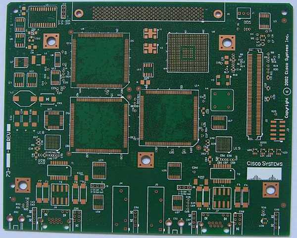
High Density Interconnect PCB from Hitech Circuits
HDI pcb is the abbreviation for High Density Interconnect pcb or High Density pcb. An HDI PCB is defined as a printed circuit board with a higher wiring density per unit area than a conventional PCB. Hitech Circuits Co., Limited is a professional high density interconnect pcbs, hdi pcb board manufacturer, supplier and design company from China, if you are looking for reliable high density interconnect PCb board partner from China, please don’t hesitate to contact [email protected] . <br>What is a high-density interconnection PCB board <br>HDI is the abbreviation of High Density Interconnection, which is a kind of technology for the production of printed circuit boards. High density interconnection PCB board is a circuit board with a relatively high line distribution density using micro-blind and buried via technology. <br> <br>HDI includes the use of fine features or signal traces and spaces of 0.003” (75 µm) or less and laser-drilled blind or buried microvia technology. Microvias allow the use of micro-interconnects from one layer to another within a PCB utilizing a smaller pad diameter creating additional routing density or reducing form factor. <br> <br>HDI pcb board is a compact product designed for small-capacity users. <br> <br>Advantages of high-density interconnected PCB boards <br>It can reduce the cost of PCB: When the density of PCB increases to more than eight-layer board, it is manufactured by HDI, and its cost will be lower than that of the traditional complex pressing process. <br>Increase circuit density: has better interconnection than that of traditional circuit boards and parts <br>Conducive to the use of advanced construction technology <br>Have better electrical performance and signal accuracy <br>Better reliability <br>Can improve thermal properties <br>It can improve radio frequency interference ( RFI ), electromagnetic wave interference ( EMI ), electrostatic discharge ( ESD ) <br>Increase design efficiency <br>Disadvantages of high-density interconnected PCB boards <br>The value of NDI impedance focuses on pattern transfer (complexity of patterns) and pattern electroplating process. <br>The quantity and quality are abnormal, especially the high-density circuit part of the HDI PCB board has a slower etch rate than the isolation line, which causes the isolation line to be over-etched. <br>When the entire HDI board is etched after electroplating, a large area of copper on the PCB circuit board will be etched away, which increases the production cost. At the same time, a large amount of copper ions enter the waste liquid after etching, causing environmental pollution and difficulty in recycling. <br>High-density interconnection PCB board Vs ordinary PCB board <br>Ordinary PCB board is mainly FR-4, which is laminated with epoxy resin and electronic grade glass cloth. Generally, traditional HDI PCB board uses backed copper foil on the outer surface, because laser drilling cannot penetrate the glass cloth, glass fiber-free backed copper foil is generally used. However, the current high-energy laser drilling machine can penetrate 1180 glass cloth. This is no difference from ordinary PCB board materials. <br> <br>Applications of high-density interconnected PCB boards <br>While electronic design is constantly improving the performance of the whole equipment, researchers are also working hard to reduce its size. In small portable products ranging from mobile phones to smart weapons, “small” is an eternal pursuit. High-density interconnection (HDI PCB) technology can make terminal product designs more compact, while meeting higher standards of electronic performance and efficiency. HDI PCB board is widely used in mobile phones, digital cameras, MP3, MP4, notebook computers, automotive electronics, IC carrier boards and other digital products, among which mobile phones are the most widely used. <br> <br>High density PCB is used extensively in applications and industries including <br> <br>Cell phone <br>GPS <br>Telecom <br>Semiconductor <br>Automotive <br>Military <br>Medical <br>Instrumentation <br>Note book computers <br>IC Carrier board <br>Healthcare <br>FAQs for Hitech Circuits on HDI PCBs <br>1. What types of HDI PCBs are available at Hitech Circuits? <br>Hitech Circuits offers a range of HDI PCBs, including those with through vias from surface to surface, with buried vias and through vias, sequential lamination with various materials, and with passive substrate constructions having no electrical connection. Each type caters to specific design and performance requirements. <br> <br>2. Can Hitech Circuits accommodate custom HDI PCB designs? <br>Absolutely! Hitech Circuits specializes in custom HDI PCB designs tailored to meet unique project requirements. Our team works closely with clients to understand their needs and deliver high-quality, precise PCBs that fit their specifications. <br> <br>3. What materials are used in the manufacturing of HDI PCBs? <br>HDI PCBs at Hi-Tech Circuits are made from various high-quality materials, including FR-4, high-frequency materials (such as Rogers and Taconic), and flex and rigid-flex materials. Material selection depends on the application’s requirements, such as thermal management, electrical performance, and mechanical durability. <br> <br>4. How does Hitech Circuits ensure the quality of their HDI PCBs? <br>Quality assurance is paramount at Hitech Circuits. We employ stringent quality control processes at every manufacturing stage, from design and material selection to fabrication and testing. Our HDI PCBs undergo multiple quality checks, including electrical testing, visual inspection, and automated optical inspection (AOI) to ensure they meet the highest standards. <br> <br>5. What are the lead times for HDI PCB production? <br>Lead times for HDI PCB production can vary based on the complexity of the design and the quantity required. Generally, prototype orders can be completed within a few days to two weeks, while larger production orders may take several weeks. We strive to meet our clients’ deadlines and can provide more specific timeframes upon order placement. <br> <br>6. Are there any design guidelines for HDI PCBs I should follow? <br>Yes, Hitech Circuits provides detailed design guidelines for HDI PCBs, which include recommendations on trace width, spacing, via sizes, and layer stacking. These guidelines help ensure the manufacturability of your design and optimize performance. Our team is also available to assist with any design questions. <br> <br>7. Can Hitech Circuits support high-volume HDI PCB orders? <br>Certainly! Hitech Circuits is equipped to handle high-volume orders with the same attention to detail and quality assurance as smaller orders. We have the capacity and expertise to meet the demands of large-scale production runs efficiently. <br> <br>8. How can I get a quote for my HDI PCB project? <br>Getting a quote is easy! Visit our website, and fill out the quote request form with your project details, such as PCB specifications, quantity, and any special requirements. Our sales team will review your information and provide you with a detailed quote promptly.
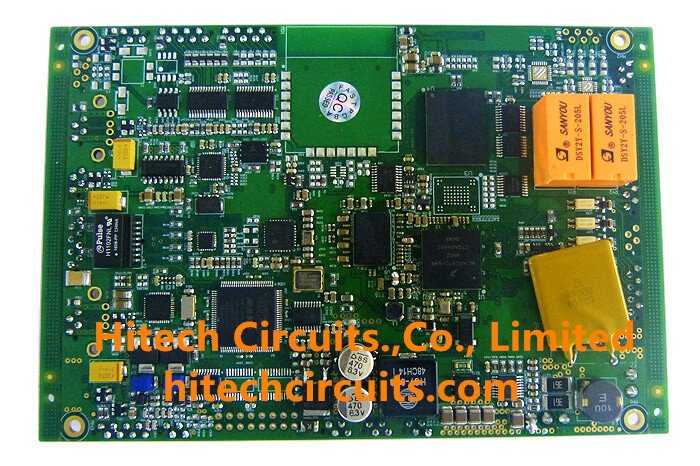
Turnkey Electronics Assembly Services
Hitech Circuits provides a full turnkey solution to all of your electronics assembly requirements. From PCB fabrication, components sourcing, pcb assembly to full box build assembly we can provide a full electronics manufacturing services solution to your electronics manufacturing requirements. Using surface mount production machinery consisting of three surface mount technology placement machines, a screen printing machine and a 10 zone reflow oven, accompanied by offline bench assembly, visual inspection and rework stations, we can offer small to medium volume services for all your pcb assembly requirements. We offer pcb assembly, visual inspection, functional and electronics testing and programming services. We can source all components, bare pcbs and production stencils. If you would like to work with an electronics manufacturer you can trust then please get in touch. <br> <br>Also, we offer both turn-key and partial turn-key PCB Electronics assembly. <br> <br>For full turn-key services, we manage and produce everything including manufacturing the circuit boards, finding & ordering PCB components, quality inspection & testing and the final product assembly. <br> <br>Advantages of Full Turnkey PCB Assembly Services <br> <br>• Shorter Lead Time <br> <br>As a fundamental form of electronic assembly, PCB assembly primarily contains three phases: PCB fabrication, components procurement and PCB assembly. Traditionally, you should quote and confirm design files with sales and engineers working for your PCB manufacturer, then components distributors and finally PCB assemblers. Such series of quotations and confirmations just need your time spent in contacting with different partners. If those partners are from different countries, you have to overcome some problems such as time zone, communication habits etc. Full-turnkey PCB assembly, however, is a highly-efficient form of electronic assembly. As soon as full-turnkey PCB assembly is determined, an overall assembly quotation and indispensible issues prohibiting smooth manufacturing will be raised so that three times of communication have been cut to one time with electronic assembly efficiency dramatically improved in Hitech Circuits Co., Limited. <br> <br>• Lower Cost <br> <br>Another advantage of full-turnkey PCB assembly service is overall cost reduction. Pack-up service is usually cheaper than separate ones as far as electronic assembly is concerned. At least, freight fee will be saved because you don’t need to get manufactured PCB boards and electronic components delivered to assembly workshop. Moreover, components procurement may get easy and customer-friendly because experienced electronic assemblers are usually able to provide reliable components with relatively low cost based on their long-term cooperation with parts manufacturers or distributors. <br> <br>• Transparent Monitoring <br> <br>When it comes to electronic assembly process, it’s significant yet difficult to monitor your products’ manufacturing stage as it is totally related with your products’ performance and time to market. Full-turnkey PCB assembly allows engineers at each stage to be aware of what they’ve accomplished and to better understand their status for better performance of final products. <br> <br>Who Can Benefit Most From Our Turnkey PCB Assembly Services? <br> <br>Now that full turnkey PCB assembly allows PCB designers to make better use of their time to focus more on PCB design, it works perfectly on companies striving for frequent upgrading and refreshing of products. They need to dig into deeper market by providing multiple creative electronic products and they strongly call for a steady and smooth electronic assembly process. <br> <br>Turnkey printed circuit board assembly is also an ideal electronic assembly solution for small businesses or startup companies that want to bring smaller quantities of assembled PCBs to market without having to invest in or carry an extensive inventory. It also offers a more cost-effective, efficient means of assembling and testing PCB prototypes for new products. In addition, quick-turn PCB assembly service makes sense for any company that needs to receive their circuit boards with the shortest possible lead time.
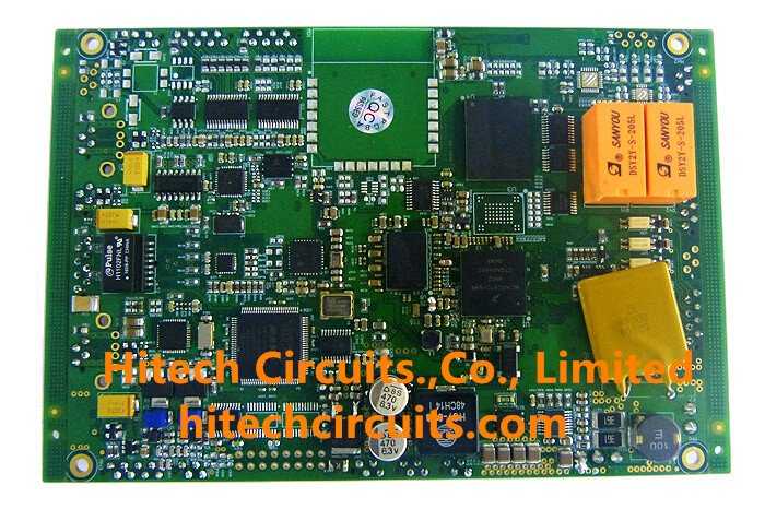
Turnkey Electronics Assembly Services
Hitech Circuits provides a full turnkey solution to all of your electronics assembly requirements. From PCB fabrication, components sourcing, pcb assembly to full box build assembly we can provide a full electronics manufacturing services solution to your electronics manufacturing requirements. Using surface mount production machinery consisting of three surface mount technology placement machines, a screen printing machine and a 10 zone reflow oven, accompanied by offline bench assembly, visual inspection and rework stations, we can offer small to medium volume services for all your pcb assembly requirements. We offer pcb assembly, visual inspection, functional and electronics testing and programming services. We can source all components, bare pcbs and production stencils. If you would like to work with an electronics manufacturer you can trust then please get in touch. <br> <br>Also, we offer both turn-key and partial turn-key PCB Electronics assembly. <br> <br>For full turn-key services, we manage and produce everything including manufacturing the circuit boards, finding & ordering PCB components, quality inspection & testing and the final product assembly. <br> <br>Advantages of Full Turnkey PCB Assembly Services <br> <br>• Shorter Lead Time <br> <br>As a fundamental form of electronic assembly, PCB assembly primarily contains three phases: PCB fabrication, components procurement and PCB assembly. Traditionally, you should quote and confirm design files with sales and engineers working for your PCB manufacturer, then components distributors and finally PCB assemblers. Such series of quotations and confirmations just need your time spent in contacting with different partners. If those partners are from different countries, you have to overcome some problems such as time zone, communication habits etc. Full-turnkey PCB assembly, however, is a highly-efficient form of electronic assembly. As soon as full-turnkey PCB assembly is determined, an overall assembly quotation and indispensible issues prohibiting smooth manufacturing will be raised so that three times of communication have been cut to one time with electronic assembly efficiency dramatically improved in Hitech Circuits Co., Limited. <br> <br>• Lower Cost <br> <br>Another advantage of full-turnkey PCB assembly service is overall cost reduction. Pack-up service is usually cheaper than separate ones as far as electronic assembly is concerned. At least, freight fee will be saved because you don’t need to get manufactured PCB boards and electronic components delivered to assembly workshop. Moreover, components procurement may get easy and customer-friendly because experienced electronic assemblers are usually able to provide reliable components with relatively low cost based on their long-term cooperation with parts manufacturers or distributors. <br> <br>• Transparent Monitoring <br> <br>When it comes to electronic assembly process, it’s significant yet difficult to monitor your products’ manufacturing stage as it is totally related with your products’ performance and time to market. Full-turnkey PCB assembly allows engineers at each stage to be aware of what they’ve accomplished and to better understand their status for better performance of final products. <br> <br>Who Can Benefit Most From Our Turnkey PCB Assembly Services? <br> <br>Now that full turnkey PCB assembly allows PCB designers to make better use of their time to focus more on PCB design, it works perfectly on companies striving for frequent upgrading and refreshing of products. They need to dig into deeper market by providing multiple creative electronic products and they strongly call for a steady and smooth electronic assembly process. <br> <br>Turnkey printed circuit board assembly is also an ideal electronic assembly solution for small businesses or startup companies that want to bring smaller quantities of assembled PCBs to market without having to invest in or carry an extensive inventory. It also offers a more cost-effective, efficient means of assembling and testing PCB prototypes for new products. In addition, quick-turn PCB assembly service makes sense for any company that needs to receive their circuit boards with the shortest possible lead time.
About PCB Assembly's Store
No description provided.
0.0
Customer Reviews
See what others are saying about PCB Assembly's Store. We verify purchases to ensure reviews are genuine.
No reviews yet for this store.