

Sandy zhou's Store
Owned by Sandy zhou Joined Feb 2024 19 Listings
Sandy zhou's Store
easyid.me/biz/sandyzhoupcba-901932 • Verified Store
Scan to open official EasyID digital store, view live catalog, or save business card.
Verified Merchant
EasyID Certified Seller
Fast 24h Packing
Direct courier dispatch
Zero Escrow Direct
Direct merchant settlement
Store Listings (2)
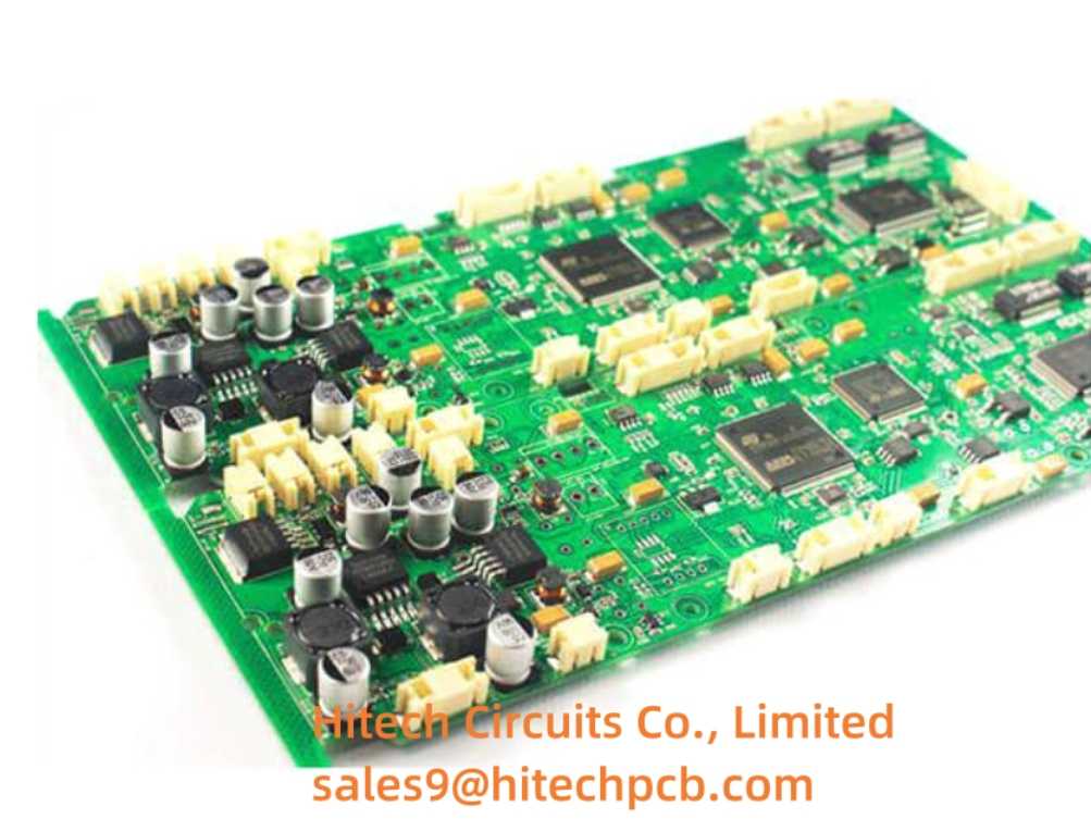
One-stop PCB Assembly Services
Turnkey generally refers to any product or service that is sold to the buyer in a immediate using form. When applied to pcb assembly, turnkey means that the supplier handles all aspects of pcb solutions, including components procuring and pcb manufacturing, picking and placing components on specific locations. In essence, full turnkey PCB assembly gives the buyer greater freedom to focus on pcb design, while the supplier takes care of the rest, which is why it is a leading form of pcb one-stop electronic assembly services. <br> <br>Technical Parameters <br>PCB Assembly China, PCB Assembly Manufacturing, quote/order 24 hour; <br>SMT Assembly, Through Hole PCB Wave soldering Assembly, Assembly services, <br>SMT Assembly Electronic assembly Manufacturing services, Mass Production <br> <br>pcb assembly china, contract electronic circuit assembly,PCBA assembly services company Shenzhen, SMT assembly EMS/OEM <br> <br>PCB Assembly mass Production: <br>SMT, Though hole components, PCBA circuit boards assembly. <br>For furhter information, please feel free to contact us: [email protected] .
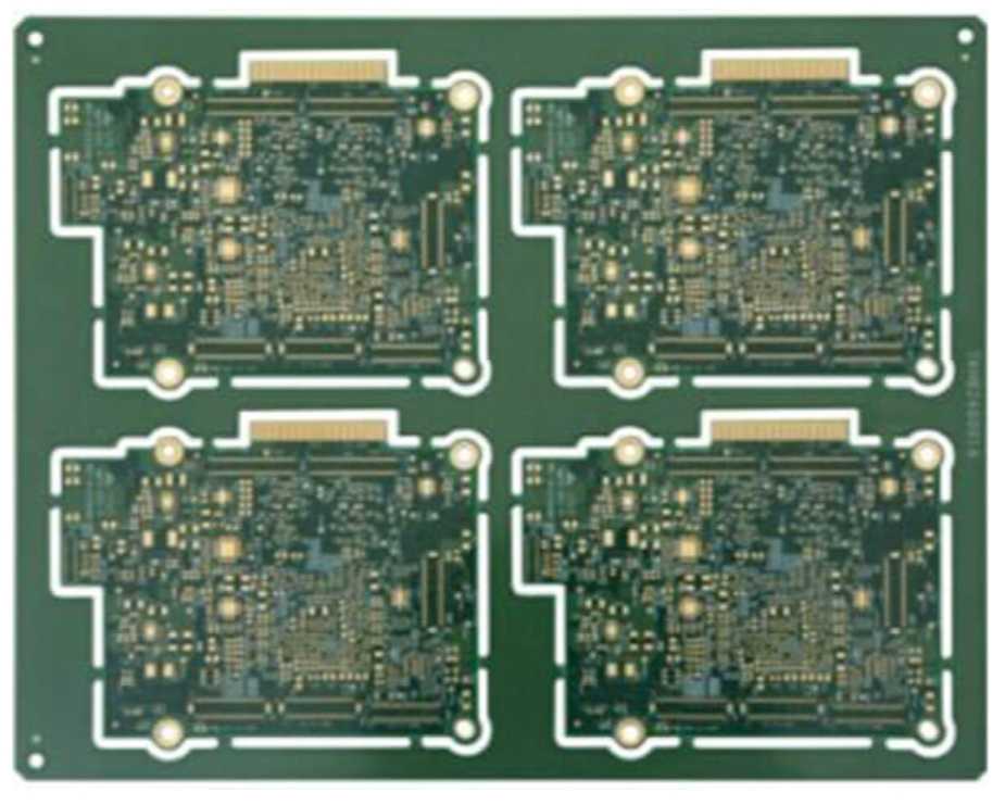
High Density Interconnect PCB China (24 layers)
24 layers high density interconnect pcb (HDI PCB) can meet higher component density and smaller packaging requirements. Through the heat conduction channel and the solid-liquid phase change cavity, the temperature of the circuit board can be effectively reduced, and the service life of the pcb laminate can be improved. The pcb used to reduce size and weight, as well as to enhance electrical performance. Hitech’s high density interconnect pcb mainly uses in cell, Mp3 player, GPS, memory card, PDA, portable game console etc. <br>24 layers High Density Interconnect PCB, HDI PCB Manufacturing HDI board China <br> <br>High Density Interconnects (HDI PCB) Board are used to meet the market demand for complex designs in smaller form factors across the majority of market segments, (Wireless, Telecom, Military, Medical, Semiconductor, and Instrumentation). <br> <br>HDI Circuit boards, one of the fastest growing technologies in PCBs, HDI Boards contain blind and/or buried vias and often contain microvias of .006 or less in diameter.They have finer lines and spaces always = <3mil They have a higher circuitry density than traditional circuit boards. <br> <br>Hitechpcb maintains years of experience with HDI products and was a pioneer of second generation microvias. Now offer an entire family of microvia technology solutions for your next generation products. <br> <br>HDI Board General Information <br> <br>High Density Interconnects (HDI) board are defined as a board (PCB) witha higher wiring density per unit area than conventional printed circuit boards (PCB). They have finer lines and spaces (<100 µm), smaller vias (<150 µm) and capture pads (<400 µm), I/O>300, and higher connection pad density (>20 pads/cm2) than employed in conventional PCB technology. <br> <br>HDI board is used to reduce size and weight, as well as to enhance electrical performance. According to layer up different, currently DHI board is divided into three basic types: <br> <br>1) HDI PCB (1+N+1)HDI PCB, High Density Interconnect PCB Features: Suitable for BGA with lower I/O counts Fine line, microvia and registration technologies capable of 0.4 mm ball pitch Qualified material and surface treatment for Lead-free process Excellent mounting stability and reliability Copper filled viaHDI PCB, High Density Interconnect PCB Application: Cell , UMPC, MP3 Player, PMP, GPS, Memory Card1+N+1 HDI PCB Structure: <br> <br>2) HDI PCB (2+N+2)HDI PCB, High Density Interconnect PCB Features: Suitable for BGA with smaller ball pitch and higher I/O counts Increase routing density in complicated design Thin board capabilities Lower Dk / Df material enables better signal transmission performance Copper filled viaHDI PCB, High Density Interconnect PCB Application: Cell , PDA, UMPC, Portable game console, DSC, Camcorder <br> <br>HDI PCB Capabilities <br>Layers3 – 36 Layers <br>HDI Step 3+N+3 <br>Min.Line Width0.05mm (2 mil) <br>Min.Line Space0.05mm (2 mil) <br>Min.Annular ring0.1mm (4 mil) <br>Min. Via0.1mm (4 mil) <br>Max.Size500mm X 800mm <br>MaterialFR4,High Tg220 <br>Material thickness Start at 25um Plus copper <br>Copper thickness0.3 OZ to 10 OZ (10um – 350um) <br>[a]https%3A%2F%2Fhitechcircuits.com%2Fproduct%2Fhigh-density-interconnect-pcb-china%2F[/a] <br>If you want know more information pls contact sales9 at hitechpcb.com
About Sandy zhou's Store
No description provided.
0.0
Customer Reviews
See what others are saying about Sandy zhou's Store. We verify purchases to ensure reviews are genuine.
No reviews yet for this store.