

Sandy zhou's Store
Owned by Sandy zhou Joined Feb 2024 19 Listings
Sandy zhou's Store
easyid.me/biz/sandyzhoupcba-901932 • Verified Store
Scan to open official EasyID digital store, view live catalog, or save business card.
Verified Merchant
EasyID Certified Seller
Fast 24h Packing
Direct courier dispatch
Zero Escrow Direct
Direct merchant settlement
Store Listings (19)
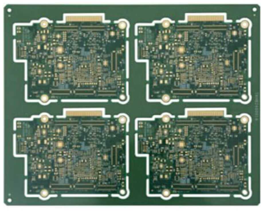
High Density Interconnect PCB China (24 layers)
24 layers high density interconnect pcb (HDI PCB) can meet higher component density and smaller packaging requirements. Through the heat conduction channel and the solid-liquid phase change cavity, the temperature of the circuit board can be effectively reduced, and the service life of the pcb laminate can be improved. The pcb used to reduce size and weight, as well as to enhance electrical performance. Hitech’s high density interconnect pcb mainly uses in cell, Mp3 player, GPS, memory card, PDA, portable game console etc. <br>24 layers High Density Interconnect PCB, HDI PCB Manufacturing HDI board China <br> <br>High Density Interconnects (HDI PCB) Board are used to meet the market demand for complex designs in smaller form factors across the majority of market segments, (Wireless, Telecom, Military, Medical, Semiconductor, and Instrumentation). <br> <br>HDI Circuit boards, one of the fastest growing technologies in PCBs, HDI Boards contain blind and/or buried vias and often contain microvias of .006 or less in diameter.They have finer lines and spaces always = <3mil They have a higher circuitry density than traditional circuit boards. <br> <br>Hitechpcb maintains years of experience with HDI products and was a pioneer of second generation microvias. Now offer an entire family of microvia technology solutions for your next generation products. <br> <br>HDI Board General Information <br> <br>High Density Interconnects (HDI) board are defined as a board (PCB) witha higher wiring density per unit area than conventional printed circuit boards (PCB). They have finer lines and spaces (<100 µm), smaller vias (<150 µm) and capture pads (<400 µm), I/O>300, and higher connection pad density (>20 pads/cm2) than employed in conventional PCB technology. <br> <br>HDI board is used to reduce size and weight, as well as to enhance electrical performance. According to layer up different, currently DHI board is divided into three basic types: <br> <br>1) HDI PCB (1+N+1)HDI PCB, High Density Interconnect PCB Features: Suitable for BGA with lower I/O counts Fine line, microvia and registration technologies capable of 0.4 mm ball pitch Qualified material and surface treatment for Lead-free process Excellent mounting stability and reliability Copper filled viaHDI PCB, High Density Interconnect PCB Application: Cell , UMPC, MP3 Player, PMP, GPS, Memory Card1+N+1 HDI PCB Structure: <br> <br>2) HDI PCB (2+N+2)HDI PCB, High Density Interconnect PCB Features: Suitable for BGA with smaller ball pitch and higher I/O counts Increase routing density in complicated design Thin board capabilities Lower Dk / Df material enables better signal transmission performance Copper filled viaHDI PCB, High Density Interconnect PCB Application: Cell , PDA, UMPC, Portable game console, DSC, Camcorder <br> <br>HDI PCB Capabilities <br>Layers3 – 36 Layers <br>HDI Step 3+N+3 <br>Min.Line Width0.05mm (2 mil) <br>Min.Line Space0.05mm (2 mil) <br>Min.Annular ring0.1mm (4 mil) <br>Min. Via0.1mm (4 mil) <br>Max.Size500mm X 800mm <br>MaterialFR4,High Tg220 <br>Material thickness Start at 25um Plus copper <br>Copper thickness0.3 OZ to 10 OZ (10um – 350um) <br>[a]https%3A%2F%2Fhitechcircuits.com%2Fproduct%2Fhigh-density-interconnect-pcb-china%2F[/a] <br>If you want know more information pls contact sales9 at hitechpcb.com
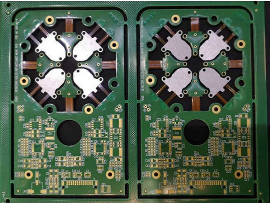
Rigid flex PCB board fabrication
Rigid-flex PCB board, it is a circuit board that combines flexible and rigid circuit board technology in the application. Most rigid-flex boards are composed of multiple layers of flexible circuit boards, which are attached to one or more rigid boards from the outside and/or from the inside, depending on the design of the application. <br>Technical Parameters <br>Product type: Rigid-flex PCB 4 layers <br>Material: PI + FR4 <br>Application filed: Electronics Equipment <br>Layer/thickness: 8L/0.127mm <br>Surface treatment: Immersion gold(ENIG) <br>Line space/width: 0.15/0.15mm <br>Minimum hole size: 0.35mm <br>Technical Feature: Special materials, <br>Rigid flex PCB technology <br>[a]https%3A%2F%2Fhitechcircuits.com%2Fproduct%2Frigid-flex-pcb-board-fabrication%2F[/a] <br>If you want know more information pls contact sales9 at hitechpcb.com
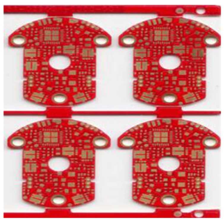
Power PCB board 6 Layers
Power pcb board, 6 layers heavy copper pcb with immersion gold surface finishing, due to their heavy copper design, the pcb is good than other circuit boards. Lightweight structure, excellent electrical performance, improve the durability of pcb, these are particularly beneficial for power devices. <br>[a]https%3A%2F%2Fhitechcircuits.com%2Fproduct%2Fpower-pcb-board-6-layers%2F%0ATechnical[/a] Parameters <br>6L Heavy copper PCB <br>Layer: 6L <br>Material: FR-4 Tg150 <br>Size: 70.8*76.2mm <br>Board thickness: 2.0mm <br>Surface finished: Immersion gold <br>Copper thickness: Inner layer 3 Oz, out layer, 3Oz <br>Min through hole: 0.6mm <br>Position control systems <br>If you want know more information pls contact sales9 at hitechpcb.com
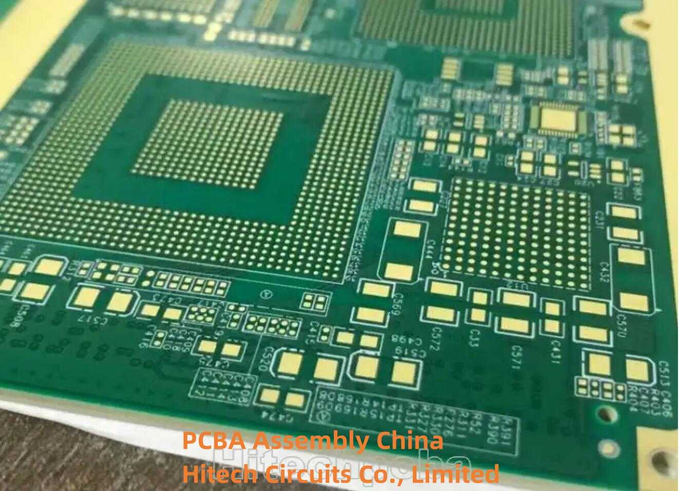
HDI PCB & High Interconnect PCB Manufacturing
The HDI board is based on the traditional double panel as the core board, which is made by continuously accumulating. This circuit board made by a continuous layer is also called the Build-Up Multilayer (BUM). Compared with the traditional circuit board, the HDI circuit board has the advantages of "light, thin, short, small". <br> <br>The electrical connection between HDI's plate layer is achieved by conductive pores, buried holes, and blind holes. Its structure is different from ordinary multi -layer circuit boards. A large number of blind holes are used in HDI boards. HDI PCB uses laser direct drilling, and standard PCB usually uses mechanical drilling, so the number of layers and high width ratio often decreases. <br> <br>HDI includes the use of fine features or signal traces and spaces of 0.003” (75 µm) or less and laser-drilled blind or buried microvia technology. Microvias allow the use of micro-interconnects from one layer to another within a PCB utilizing a smaller pad diameter creating additional routing density or reducing form factor. <br>High-density interconnect (HDI) PCBs are characterized by finer lines, closer spaces, and more dense wiring, which allow for a faster connection while reducing the size and bulk of a project. These boards also feature blind and buried vias, laser ablated microvias, sequential lamination, and via in-pads. As a result, a HDI board can house the functionality of the previous boards used. HITECH CIRCUITS is an HDI PCB manufacturer and provider in Shenzhen, China supports HDI PCB prototype and mass production with less expensive price and quick-turn lead time. Customers from a variety of industries we serve have a common that have high expectations in quality, reliability and on-time delivery in HDI PCB production. Our quality is not afterthought, but built into each process from front-end to fabrication and shipping. <br> <br>HDI PCB's Advantages <br> <br> <br>1. Reduce PCB cost: When the density of PCB increases beyond the eight-layer board, it will be manufactured in HDI, and the cost will be lower than that of traditional complicated press-forming process. <br> <br>2. Better reliability: Due to the thin thickness and the aspect ratio of 1:1, the micropores have higher reliability when transmitting signals than ordinary through holes. <br> <br>3. Improves thermal properties: The insulating dielectric material of the HDI board has a higher glass transition temperature (Tg) and therefore has better thermal properties. <br> <br>4. Improve RF interference / electromagnetic interference / electrostatic discharge (RFI / EMI ) <br> <br>5. Increase design efficiency: Micro-hole technology allows the circuit to be arranged in the inner layer, so that the circuit designer has more design space, so the efficiency of the line design can be higher.
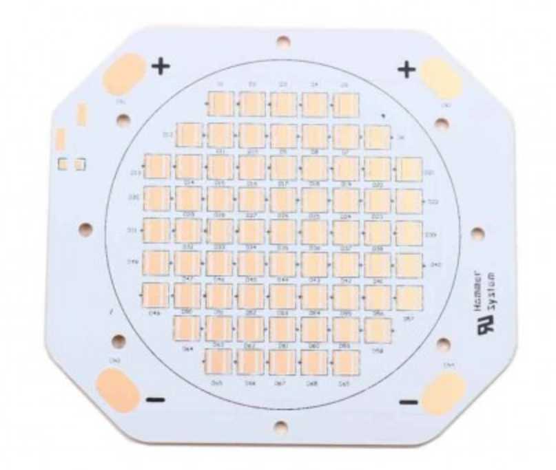
LED PCB Design
What are LEDs PCB board and LED PCB designs? <br> <br> <br> <br>LED is an acronym for light emitting diode, which is semiconductor diodes. The LED is soldered to the printed circuit board and features a chip that creates the light as electrically connected. A thermal heat sink and a ceramic base are used to bond the chip. Needless to say, LED PCB is the core of LED lighting, and an LED PCB is easy to create a high volume of heat, but making it hard to cool with traditional methods. So metal core PCB is widely used in LED application because of their enhanced ability to dissipate heat, especially aluminum is often used to fabricate PCB for LED lights. In general, the aluminum PCB contains a thin layer pf thermally conductive dielectric material that can transfer and dissipate the heat with much greater efficiency than a traditional rigid PCB. <br> <br> <br> <br>Now SMD packaging type is the most widely used packaging form in LED applications. In general, it’s limited for the light emitted from a single LED component. So multiple LED components would be used for a single light fixture to achieve sufficient light. Like other semiconductor devices, PCB is the best method to electrically connect the LED components. And a PCB with LED components soldered is usually called as “LED PCB”. <br> <br> <br> <br>LED PCB Board <br> <br>The advantages of LED PCB <br> <br> <br> <br>With the electronic products is more and more smaller and thinner, making it popular to use LED PCB, and there are various advantages with using LED PCB as follows: <br> <br>· Lightweight, low profile <br> <br>· dimensional stability <br> <br>· thermal expansion <br> <br>· heat dissipation <br> <br>· Lower cost backlit membrane switch <br> <br>· Dust and moisture resistant <br> <br>· Make it easy to integrate into complex interface assemblies <br> <br>· Efficient low power consumption <br> <br>· Available in a wide variety of sizes, colors, and intensities <br> <br>· May be used in silver flex membrane switches and copper flex membrane switches. <br> <br> <br> <br>There are two main reasons which make the LED PCB be popular in addition to increasing the light output of the fixture with integrating multiple LED components. <br> <br>1. It’s easy to tune the color function by integrating the LED components with different color temperatures or different colors into the same PCB. <br> <br>2. It can achieve the various light fixtures to meet different lighting requirements with the boards that have different shapes, sizes and materials. <br> <br> <br> <br>The LED lighting industry <br> <br> <br> <br>LED lighting or light emitting diode is an increasingly popular lighting solution, so it’s popular to improve longevity and reduce environmental impact. There are some benefits of LED lighting for traditional methods as follows: <br> <br>Lower power consumption: great LED lights with high quality can be six to seven times more efficient than traditional incandescent lights. On average, switching your home from incandescent lighting to LED lights can cut your energy use by more than 80 percent. <br> <br>Longer Lifespan: LED light bulbs can have a life of over 25,000 hours, or three years of 24/7 use, which is 25 times longer than any traditional light bulb. So it saves you the time, money and effort involved in purchasing and installing new bulbs. <br> <br>More Efficient: Traditional incandescent light bulbs release 90 percent or more of their energy as heat. LED lights cut this by up to twenty percent. It means more of your energy is going into lighting your home, and less into unnecessarily heating it. <br> <br>Very Compact: LED lights have various sizes and types in applications due to their small size. It means manufacturers can insert LEDs into anything from computers and smartphones to cars and traffic lights. <br>Mercury Free: LED lights contain no mercury, unlike more traditional options. So LEDs have a smaller environmental impact than traditional bulbs and can be more easily disposed of, without special disposal procedures. <br>[a]https%3A%2F%2Fwww.hitechpcba.com%2Fled-pcb-design[/a] <br>If you want know more information pls contact sales9 at hitechpcb.com
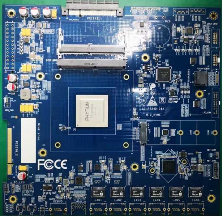
Box Build Assembly & Electronic Manufacturing Supplier
Hitech is a 10+ years experience electronic & PCB manufacturer in China, we supplies PCB board for technology startups. Email [email protected] whether you want to assemble and test prototypes or small batches of PCB boards. <br>Technical Parameters <br>Fully Automated Screen Printers with 2-D vision. <br>Inline 3-D Solder Paste Inspection (SPI). <br>Fully Automated Pick and Place Equipment capable of placing 01005 chip components and micro-BGA’s. <br>Automated Optical Inspection (AOI) is performed on all surface mount components. <br>Off line programming and quick change feeders allow for the utmost efficiency and flexibility in job change over. <br>3-D X-Ray for BGA and QFN components. <br>Quick-change feeders for job flexibility. <br>Dedicated lead and lead-free Selective Solder and Wave Solder equipment. <br>Send An Inquiry <br>Product Name: <br>Electronics manufacturing company <br>Product URL: <br>[a]https%3A%2F%2Fhitechcircuits.com%2Fproduct%2Felectronic-manufacturing-company%2F[/a]
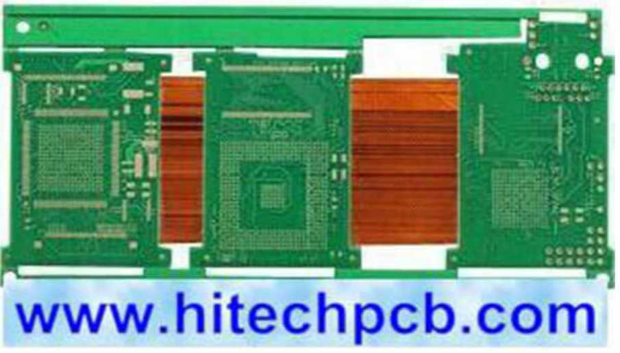
Rigid flex PCB board fabrication
Rigid-flex PCB board, it is a circuit board that combines flexible and rigid circuit board technology in the application. Most rigid-flex boards are composed of multiple layers of flexible circuit boards, which are attached to one or more rigid boards from the outside and/or from the inside, depending on the design of the application. <br>Technical Parameters <br>Product type: Rigid-flex PCB 4 layers <br>Material: PI + FR4 <br>Application filed: Electronics Equipment <br>Layer/thickness: 8L/0.127mm <br>Surface treatment: Immersion gold(ENIG) <br>Line space/width: 0.15/0.15mm <br>Minimum hole size: 0.35mm <br>Technical Feature: Special materials, <br>Rigid flex PCB technology <br>Send An Inquiry <br>Product Name: <br>Rigid flex PCB board fabrication <br>Product URL: <br>[a]https%3A%2F%2Fhitechcircuits.com%2Fproduct%2Frigid-flex-pcb-board-fabrication%2F[/a]
About Sandy zhou's Store
No description provided.
0.0
Customer Reviews
See what others are saying about Sandy zhou's Store. We verify purchases to ensure reviews are genuine.
No reviews yet for this store.