

Cynthia_HitechPCB_manufacturing Hitech Circuits PCB's Store
Owned by Cynthia_HitechPCB_manufacturing Hitech Circuits PCB Joined Mar 2024 20 Listings
Cynthia_HitechPCB_manufacturing Hitech Circuits PCB's Store
easyid.me/biz/cynthia-hitechpcb-manufacturing-49b759 • Verified Store
Scan to open official EasyID digital store, view live catalog, or save business card.
Verified Merchant
EasyID Certified Seller
Fast 24h Packing
Direct courier dispatch
Zero Escrow Direct
Direct merchant settlement
Store Listings (20)
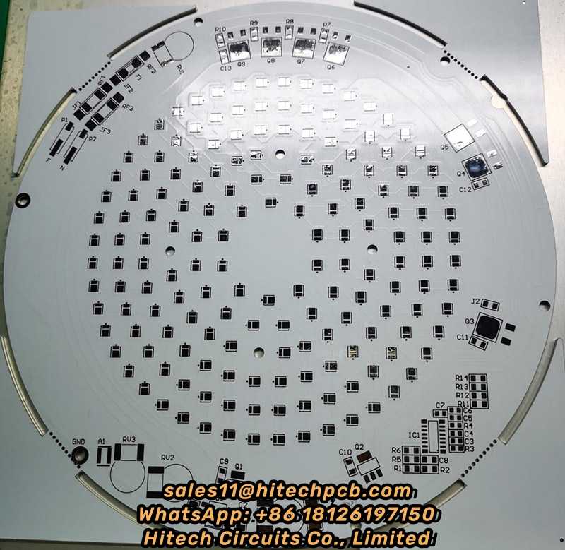
Aluminium PCB – Hitech Circuits Co., Limited, from China
Aluminium PCB – Hitech Circuits Co., Limited, from China <br> <br>1. What’s Aluminium LED PCB? <br>Aluminum LED PCB substrate is a metal - based copper-clad sheet with good heat dissipation. A single panel is generally composed of three layers of structure, namely the circuit layer (copper foil), insulation layer and metal base layer. It is commonly found in LED lighting products. There are two sides, the white side is used to weld the LED pins, and the other side is the natural color of aluminum, which is usually coated with heat-conducting gel and then in contact with the heat-conducting part. Among all metal core PCBS, Aluminum LED PCB is the most common type. The base material consists of an aluminum core and standard FR4. It features a thermal cladding that dissipates heat in an efficient manner while cooling components and improving the overall performance of the product. Currently, aluminum-backed PCBS are considered solutions for high power and tight tolerance applications. <br> <br> <br>2. Aluminum LED PCB with Copper Layer, Dielectric Layer & Aluminum Layer <br>Aluminum LED PCB has a similar layout to any other printed circuit boards with copper layer(s), solder mask layer(s) and silkscreen(s). Instead of having a fiberglass or plastic substrate, Aluminum LED PCB is made from metal core substrate, which consists of copper layer, dielectric layer and aluminum layer. This substrate is called as Aluminum based copper clad laminate (CCL). The glass reinforced and ceramic filled dielectric layer in-between copper layer and aluminum layer is very thin, but plays a very important role of electric insulation and thermal conductivity (because of minimum thermal resistance) from copper layer to aluminum base. The copper is etched into conductors and metal base is to withdraw thermal (/heat). The superior heat transfer capacity of Aluminum-based PCB helps cooling components while eliminating problems associated with managing fragile ceramics. <br> <br> <br>3. Thermal conductivity of Aluminium LED PCB <br>The general thermal conductivity of Aluminum LED PCB is 0.3, 0.6, 1.0, 1.5, 2.0, 3.0, 5.0, 122W/m.k, etc., among which 0.3-1.0w /m.k is the general conductive Aluminum LED PCB, 1.5W/m.k is the middle conductive Aluminum LED PCB, 2.0-3.0w /m.k is the high conductive Aluminum LED PCB. 5.0W/m.k is thin abasal substrate, and 122W/m.k is ultra-high conductivity Aluminum LED PCB, also known as ALC Aluminum LED PCB. <br> <br>At present, the common Aluminum LED PCB on the market has a thermal conductivity of 1.0, 1.5, 2.0W/m.k high conductivity type Aluminium LED, wherein the thermal conductivity of 1.0W/m.k Aluminum LED PCB is called general Aluminum LED PCB, its insulation layer is composed of epoxy glass cloth bonded sheet; Aluminum LED PCB with thermal conductivity of 1.5W/m.k is called high heat dissipation Aluminum LED PCB, and its insulation layer is composed of epoxy resin or other resins with high thermal conductivity; The Aluminum LED PCB with a thermal conductivity of 2.0W/m.k is called the Aluminum LED PCB for high-frequency circuit, and the insulating layer is composed of polyolefin resin or Polyimide resin glass cloth bonded sheet. The thermal conductivity of Aluminum LED PCB varies according to the copper layer in the circuit. Different processes produce different levels of thermal conductivity. <br> <br>We currently support Aluminum based CCLs from Ventec, GDM and BoYu with thermal conductivity from 1.0 ~ 7 W/m•K. The Aluminum LED PCB prices of Ventec is much higher than that with GDM and BOYU since material cost, and the prices of high thermal conductivity is higher than low thermal conductivity. Hitechpcb provides a wide range of electrical and thermally conductive interface pads, thermally conductive gap filler, thermal phase change materials and thermally conductive electrically insulating materials, as well as specialized equipment for high volume Aluminum LED PCB manufacturing. Choosing Hitech Circuits PCB as your Aluminum LED PCB supplier, just send your Gerber files and fabrication notes to us, we will deliver qualitied PCB boards to you on time. <br> <br> <br>4. Dielectric Constant of Aluminium LED PCB <br>The dielectric constant of Aluminum LED PCB substrate is a special detection method for Aluminum LED PCB. It is a variable Q value series resonance method through the measurement of dielectric constant and dielectric loss factor. The sample and tuning capacitor are connected in series to the high frequency circuit to measure the series circuit The principle of Q value. <br> <br>The performance of Aluminum LED PCB includes requirements such as peel strength, surface resistivity, minimum breakdown voltage, dielectric constant, flammability and thermal resistance. <br> <br> <br>5. Aluminum LED PCB with White Solder Mask <br>The retail price of Aluminum LED lights has dropped dramatically in recent years, while the energy efficiency and brightness of LED lights have improved. These technological advances have led some to predict annual growth of 45% over the next five years. With the development of the LED industry, the demand for LED PCBS and solder masks is also increasing. Solder shield is a protective coating applied to exposed printed circuit boards. The exposed PCB board is covered with a mask to prevent accidental solder bridging during PCB assembly and to protect the PCB from the environment. Solder masks are traditionally green, and are expected to withstand the high temperatures that occur in reflow soldering, as different colors such as blue, red, or black will occasionally appear. Increased production of Hitch Aluminum LED PCB requires increased whiteness and color stability of the mask. Aluminum LED PCB commonly used LPI welding color is white and black, of which white welding color is the most commonly used to achieve high brightness and perfect light reflection. White Aluminum LED PCB ensures no darkening and will not affect the color temperature of LED smd. At the same time, it also helps to increase the life of LED applications. Looking for reliable Aluminum LED PCB suppliers, Hitech is a good choice. <br> <br> <br>6. Classification of Aluminum LED PCB Substrate <br>Aluminum LED PCB-based copper clad plates are divided into three categories: <br> <br>The first is the universal aluminum-based copper clad plate, the insulation layer is composed of epoxy glass cloth bonded sheet; <br> <br>The second is the high heat dissipation aluminum-based copper-clad plate, the insulation layer is composed of high thermal conductivity epoxy resin or other resins; <br> <br>Third, high frequency circuit aluminum base copper plate, insulation layer by polyolefin resin or Polyimide resin glass cloth bonded sheet. <br> <br>The biggest difference between aluminum clad copper plate and conventional FR-4 clad copper plate is heat dissipation. Compared with 1.5mm thickness of FR-4 clad copper plate and aluminum clad copper plate, the former thermal resistance of 20 ~ 22 ℃, the latter thermal resistance of 1.0 ~ 2.0℃, the latter is much smaller. <br> <br>7. Aluminum LED PCB Performance: <br>(1) Heat dissipation <br>Many double panel, multi - layer plate high density, power, heat distribution is difficult. Conventional printed board substrates such as FR4, CEM3 are bad conductors of heat, insulation between layers, heat does not escape. Local heating of electronic equipment is not excluded, leading to high temperature failure of electronic components, and Aluminum LED PCB can solve this problem of heat dissipation. <br> <br>(2) Thermal Expansibility <br>Thermal expansion and cold contraction is the common nature of substances, and the coefficient of thermal expansion of different substances is different. Aluminum based printed board can effectively solve the problem of heat dissipation, so that the printed board components of different substances on the thermal expansion and contraction problem, improve the durability and reliability of the whole machine and electronic equipment. Especially solve SMT (surface mount technology) thermal expansion and shrinkage problems. <br> <br>(3) Dimensional stability <br>Aluminum-based printed boards are obviously much more stable in size than those made of insulating materials. Aluminum base printed board, aluminum sandwich board, heating from 30℃ to 140~150℃, the size change is 2.5~3.0%. <br> <br>(4) Other reasons <br>Aluminum based printed board, with shielding effect; Instead of brittle ceramic substrate; Safe use of surface mounting technology; Reducing the real effective area of the printed board; Instead of radiator and other components, improve the heat resistance and physical properties of products; Reduce production costs and labor. <br> <br> <br>8. Why choose Aluminum LED PCB from Hitechpcb? What are the advantages of Aluminum LED PCB? <br>(1) Good heat dissipation performance: Aluminum LED PCB can reduce the thermal resistance to the minimum, has a smaller thermal resistance, thermal expansion coefficient is closer to copper foil, so that Aluminum LED PCB has excellent thermal conductivity and heat dissipation performance, reduce the module operating temperature, prolong the service life. <br> <br>High current load: Using the same thickness, the same line width, Aluminum LED PCB substrate can carry higher current. <br> <br>(2) Good machinability: can replace ceramic substrate, better mechanical endurance. At the same time, high strength and toughness, can realize large area printed board manufacturing and component mounting. <br> <br>(3) Good electromagnetic shielding: In order to ensure the performance of electronic circuits, some components of electronic products need to prevent electromagnetic radiation and interference. Aluminum LED PCB can act as a shield plate, play the role of shielding electromagnetic wave <br> <br>(4) Environmental protection: The Aluminum LED PCB used in the raw material is non-toxic and can be recycled. Meet RoHs requirements. <br> <br>(5)Light weight: Aluminum LED PCB has a surprisingly light weight with excellent strength and elasticity, which is very convenient. <br> <br>Hitech Circuits can provide high quality and affordable Aluminum LED PCB products for you. <br> <br> <br>9. Technical requirements for Aluminum LED PCB <br>The main technical requirements are: <br>1. Dimensional requirements: including panel size and deviation, thickness and deviation, perpendicularity and warpage; Appearance, including cracks, scratches, burrs and delimitation, aluminum oxide film, etc. <br> <br>2. Performance requirements, including peel strength, surface resistively, minimum breakdown voltage, dielectric constant, combustion and thermal resistance requirements. <br> <br> <br>10. Special test method for Aluminum-based copper clad plates <br>One is the measurement method of dielectric constant and dielectric loss factor. It is the series resonance method with variable Q value. The sample and tuned capacitor are connected to the high-frequency circuit in series to measure the Q value of the series circuit. <br> <br>The other is the measurement method of thermal resistance, which is calculated by the ratio of temperature difference and heat conduction between different temperature measurement points. <br> <br> <br>11. The Aluminum LED PCB manufacturing process in Hitechpcba <br>(1)Substrate cutting <br> <br>a. cutting process: material → cutting <br> <br>b. Note: ① Check the size of the first piece; ② Pay attention to Aluminum surface scratching and copper surface scratching; ③ Pay attention to the layering of the board edge and the tip. <br> <br>(2)Plate drilling <br> <br>a, drilling process: pin → drilling → inspection plate <br> <br>b, matters needing attention: ① check the number of drilling holes, the size of the empty chestnut chain; ② Check the plate burr, hole deviation; ③ Avoid scratching the substrate; ④ Check and replace the drill nozzle. <br> <br>(3) Imaging transfer <br> <br>a, graphic imaging process: grinding plate → film → exposure → development <br> <br>b, precautions: ① Check whether there is an open circuit after development; ② Pay attention to the poor line caused by the board wipe; ③ There can be no air residual exposure to prevent poor exposure; ④ Whether there is deviation in developing counterpoint; ⑤ After exposure, the development should be done at rest for more than 15 minutes. <br> <br>(4)Solder mask and Silkscreen process <br> <br>a, kill row silk printing resistance welding, character process: screen printing → pre-baking → exposure → development → character <br> <br>b, matters needing attention: ① Check whether there is foreign body on the board; ② Pay attention to the cleaning of the net board; ③ Pre-bake for more than 30 minutes after screen printing, to avoid bubbles in the line; ④ Pay attention to the thickness and uniformity of screen printing; ⑤ After the pre-baked plate to completely mutual cooling, avoid touching film or damage to the ink surface gloss. <br> <br>(5)E-test or flying probe test <br> <br>a, test process: line test → withstand voltage test <br> <br>b, precautions: ① How to distinguish after the test how to store qualified and unqualified products. <br> <br>(6)FQC, FQA, packaging, shipping <br> <br>a. Process: FQC→FQA→ Packaging → shipping <br> <br>b. Note: ① FQC should pay attention to the confirmation of the appearance of the finished Aluminum LED PCB in the process of eye inspection and make a reasonable distinction; ② FQA does spot check and verify the inspection standards of FQC; ③ We should confirm the number of packages to avoid mixed plates, wrong plates and package <br> <br> <br>12. Application of Aluminum LED PCB <br>1. Audio devices: input, output amplifier, balance amplifier, audio amplifier, preamplifier, power amplifier. <br> <br>2. Power Supply: switching voltage regulator, DC/AC converter, SW voltage regulator, etc. <br> <br>3. Communication electronic equipment: high frequency amplifier, filter, transmitter circuit <br> <br>4. Office automation equipment: motor drive, etc <br> <br>5. Automobile: electronic regulator, ignition device, power controller, etc. <br> <br>6. Computer :CPU board, floppy disk drive, power equipment, etc. <br> <br>7. Power module: converter, solid relay, rectifier bridge, etc <br> <br>8. Lamps and lighting: A variety of colorful LED energy-saving lamps are well received by the market, and Aluminum LED PCB used in LED lights has also begun to be applied on a large scale. <br> <br>13. Aluminum LED PCB Storage Conditions <br>Aluminum LED PCB are generally stored in a dark and dry environment. Most Aluminum LED tube lighting metal core pcb are prone to dampness, yellowing, and blackening. Generally, they should be used within 48 hours after opening the vacuum package. <br> <br>14. Specification for the manufacture of Aluminum LED PCB <br>a. Aluminum LED PCB is often used in power devices, power density is high, so the copper foil is thicker. If copper foils over 3oz are used, the etching of thick copper foils requires engineered line width compensation, otherwise the line width will be out of tolerance after etching. <br> <br>b. The aluminum base surface of aluminum substrate must be protected by protective film in advance during PCB processing, otherwise, some chemicals will etch the aluminum base surface, resulting in appearance damage. And the protective film is easy to be hurt, resulting in gaps, which requires the whole PCB processing process must be inserted. <br> <br>c. The hardness of the milling cutter used by the glass fiber board gong board is relatively small, and the hardness of the milling cutter used by the aluminum substrate is large. In the process of manufacturing glass fiber board milling cutter speed, while the production of aluminum substrate is at least two thirds slower. <br> <br>d, computer milling glass fiber board is just the use of the machine's own cooling system, but the processing of aluminum substrate must be in addition to alcohol heat dissipation for the gong head. <br> <br>15. Aluminum LED PCB circuit fabrication <br>(1) Mechanical processing: Drilling of aluminum substrate can be done, but no burr is allowed on the edge of the inner hole after drilling, which will affect the pressure test. Milling the shape is very difficult. And punching shape, need to use advanced mold, mold production is very skilled, as one of the difficulties of aluminum substrate. After shape punching, the edge should be very neat, without any burr, and do not hurt the welding resistance layer on the edge of the plate. Usually the use of soldier die, hole from the line, shape from the aluminum surface, circuit board punching force is cut down, and so on are skills. After punching the shape, the warpage of the board should be less than 0.5%. <br> <br>(2) The whole production process is not allowed to wipe the aluminum base surface: aluminum base touch, or by a certain chemical will produce surface discoloration, blackening, which is absolutely unacceptable, re-polishing aluminum base some customers do not receive, so the whole process does not touch the aluminum base surface is one of the difficulties in the production of aluminum base plate. Some enterprises use passivation process, some in hot air leveling (spray tin) before and after each pasted protective film. <br> <br>(3) Over-high voltage test: the aluminum base board of the communication power supply shall be tested at 100% high voltage. Some customers require direct current or alternating current. The voltage shall be 1500V or 1600V, and the time shall be 5 seconds or 10 seconds. Dirt on the board, holes and aluminum edge burr, line saw tooth, damage to any little insulation layer will lead to high voltage test fire, leakage, breakdown. Pressure test board stratification, foaming, are rejected. <br> <br>For further details freely contact Cynthia at [email protected] <br>[a]https%3A%2F%2Fwww.hitechpcba.com%2Faluminium-led-pcb[/a]
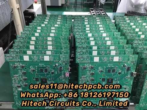
Your leading PCB High Volume PCB Assembly supplier in China
Your leading PCB High Volume PCB Assembly supplier in China <br> <br>With 15 years of experience and high efficiency in PCB assembly and manufacturing, HITECH CIRCUITS is the perfect source for Big Batch PCB assembly on a limited budget. If you are looking for a large PCBA assembly within your budget, we will be your ideal choice. HITECH CIRCUITS has more than 15 years of experience in the OEM/PCBA manufacturing and assembly of printed circuit boards, advanced production technology and equipment, professional engineers and purchasing team to provide our partners with personalized and complete process solutions. HITECH CIRCUITS’s supply chain services deliver supply chain innovation on demand. We offer a bold, yet proven service solution designed to grow market share and profit. Our innovative approach to managing the supply chain offers a complete business model that delivers the talent and transformative tools necessary to create predictability, reliability, and responsiveness across your entire supply chain. Our practitioners are passionate about supply chains. We have spent a generation understanding, refining and building the best in intelligent supply chains. We provide talent on-demand with expertise in data analytics and strategic technologies that can help you predict, plan and respond more effectively. <br> <br>Some designs require assemblies in small volume, maybe just prototypes, while others require them in high volume. At SMT house, High Volume, Large Volume, or Big Batch PCB Assembly always refers to printed board assembly projects with quantities more than 5K pieces. HitechPCB has the capability to offer high volume PCB assembly services to meet your requirements of high-quality, competitive price, on-time delivery and smooth communication in any manner of full turnkey, consigned and partial turnkey. <br> <br>Also, if your business is involved in applications that require high-volume PCB assembly, the company to contact is HitechPCB, because we’re a complete turnkey solution for printed circuit boards assembly, we are ideally suited for bulk PCB assembly orders. Our state-of-the-art equipments, large facility and wide range of highly-qualified experts give us the capability of high-volume PCB assembly of up to 9,000,000. <br> <br>We are also the perfect source if you’re looking for large-order PCB assembly on a budget. Because of our high level of efficiency and more than 10 years of experience with printed circuit board manufacturing and electronics assembly, we offer large printed circuit board orders at surprisingly competitive prices compared to other PCB manufacturers or PCB assembly companies. <br> <br>Our large order PCB assembly process starts with a tested and practiced set of workflow guidelines for every phase of the process, from pre-order PCB design consultation with professional veteran engineers to PCB fabrication, components sourcing, PCB assembly, PCBA testing, PCBA inspection, PCBA packing and shipping all under the auspices of a highly-skilled production staff. You can be confident that no matter how many circuit boards you order, you will enjoy fast service, low prices and extremely high quality. <br> <br>With our excellent after-sales service, 24 sales and technical support team, quick response service, we will be your best Big Batch PCB assembly manufacturer inChina. A wide variety of highly qualified experts <br> <br>Why choose Hitechpcba Big Batch PCB Assembly <br>Compared to our competitors, Hitechpcba offers large printed circuit board orders at very competitive prices. The risky big batch PCB assembly process begins with a set of tried and tested workflow guidelines. From ordering PCB design to component procurement, manufacturing, testing, assembly, inspection, shipping and packaging. This is all under the guidance of our highly skilled production staff. <br> <br>No matter how many boards you order, you'll love the fast response service, low cost, and surprisingly high quality. <br> <br>Whether you are seeking for product designer, electrical engineer, system integrator, manufacturer, or big batch PCB manufacturing and assembly, low cost big batch PCB housing, electronic assembly services, Hitech Circuits PCB Assembly team will be your perfect choice for big batch PCB assembly plant inChina. <br> <br>Finding Reliable High Volume PCB Assembly Supplier? <br> <br>When your design passed the prototyping verification after optimization, DFM and DFT check, it’s time to find a manufacturer or a supplier who has ability to perform high volume PCB manufacturing and assembly for you. HITECH CIRCUITS is a one-stop PCB solution provider, no matter which your design stage is located, we always can help in PCB manufacturing, assembly and design. With both design and manufacturing knowledge, we can feedback some suggestions to modify or change your design on the basis of cost-down without sacrificing the quality and performance. What’s more, if choosing our full turnkey PCB assembly service, we will be responsible of BOM sourcing to reduce your workload. Our approach to conducting high volume printed circuit board assembly is founded on a commitment to the highest possible quality, based on IPC standards and our inner quality control processes. In spirit of those high assembly standards, HITECH CIRCUITS developed excellent high-volume assembly capabilities and manufacturing processes relied on our advanced assembly lines in dust-free workshop. <br> <br> <br>What is big batch PCB assembly? <br> <br>Big batch PCB assembly is an assembly process where you will assemble 10,000 or more PCBs in a specific period of time. The main processes you will use to assemble PCBs in large quantities are design for manufacturing and design for testing. <br> <br>What are the advantages of using big batch PCB assembly? PCB assembly process <br> <br>With applications in mind, big batch PCB assembly will provide you with numerous industrial and personal benefits. This is why electronic OEM prefer to use it in most of their applications. <br> <br>The following are the main advantages of using mass printed circuit components: <br> <br>Rapid design and prototyping process <br>Since you will be mass-producing or manufacturing printed circuit boards, you must assemble them uniformly. By simply creating a design and a prototype that works for each PCB, you can save a lot of time. <br> <br>Short production cycle <br>Since the production process is fully automatic, you will also save time in the production of numerous PCBS. It all starts with the design and prototyping phase, which you'll do with the help of software and machines. <br> <br>Production consistency <br>You will also have a very uniform production process because most of the details are predetermined before implementation. Once production begins, all manufacturing specifications will follow uniform specifications for all printed circuit boards. <br> <br>Quality consistency <br>Since you will be producing all PCBs to similar specifications, you will automatically get consistent quality throughout the production process. In other words, you should rest easy knowing that you will have consistency across all printed boards. <br> <br>First-class cost performance <br>This is the most convenient model for the cost of producing printed circuit boards because you can do everything very consistently. Here, you will buy all the materials in bulk and produce them in a short time using similar machines. <br> <br>Improve the market's ability to time <br>You will be able to produce large number of printed circuit boards in a very short time, thus giving you the advantage in the market. In other words, you will have a steady supply of on-demand printed circuit boards, giving you the advantage in the market. <br> <br>Do you have lead-free mass PCB assembly? <br>Yes, we care about the health of our users and the health of the environment. We are aware of the harmful or negative effects that lead emissions can have on users and the environment.That's why we eliminate lead from production materials. It is of great benefit to protect people's health and eliminate environmental pollution. <br> <br>What is the testing protocol for mass PCB assembly? <br>As long as you have completed the process of producing printed circuit boards, you must ensure that they run well. <br> <br>Existing testing protocols will help ensure that large volumes of PCBs are in perfect working condition. <br> <br>Here are the main test protocols you can perform on a high volume printed circuit board: <br> <br>Automated Optical Inspection (AOI) <br>You will use Automated Optical Inspection (AOI) tools to accurately and efficiently detect production errors in big batch PCB assembly. It has cameras and image-processing software that can identify assembly errors and relay information for further action. It is the best tool you will use for better error detection than visual inspection. <br> <br>Solder Paste Inspection (SPI) <br>After you have finished printing with the paste printer, you must pass it through the paste inspector. The SPI machine has a camera and communication system equipment that can examine every detail of the solder paste.It compares these details to the Gerber file and reports any kind of inconsistency. <br> <br>In-Circuit Test (ICT) <br>In-Circuit Test, you can use the most detailed test methods to check the quality and integrity of the PCB.Here, you will have to take personal initiative and use online testing software to check the quality of your PCB.You will use the machine to detect errors in the PCB for correction. <br> <br>Functional Circuit Test <br>Here, you will use a computer with test pins or test probes to test the functional integrity of the PCB. You can tell if the board passes the test simply by comparing the results to the design specifications. <br> <br>X-ray Examination <br>You will use X-ray inspection to detect welding problems on the PCB that are not visible to the human eye. Here, you do not have to cut through the circuit board to see the welding quality on the printed circuit board. You'll use X-ray inspection protocols to detect errors in components and soldering on circuit boards. <br> <br>Do you have a custom mass PCB assembly? <br>Yes, we do customize mass printed circuit boards. <br>You can order the most unique types of printed circuit boards and we will produce them according to your needs. <br>We'll review your design, create a prototype, and then test how it works. <br>Once we confirm that it is working well according to the design details, we will proceed with the production process. <br> <br>How does small batch PCB assembly compare to large batch PCB assembly? <br>On the production scale, you can choose between large batch PCB assembly or small batch PCB assembly. <br>Mass PCB assembly is the process by which you assemble 10,000 or more printed circuit boards. <br>It is a mass production or assembly system that can mass produce PCBs in a short period of time. <br>On the other hand, you can choose to assemble PCBs in small batches for small scale production or assembly of PCBs. <br>In other words, you will produce a very small number of printed circuit boards of 250 or less. <br>In large and small batch PCB assembly, the assembly process will remain the same. <br>In addition, you will use similar detection techniques for high - and small-lot PCB assemblies. <br> <br>What are the main capabilities of mass PCB assembly? <br>Well, when you're looking for a good large volume PCB assembler, there are some special features. <br>This means that they must have the specific resources that you will use in the PCB assembly process. <br>The following are the main functions that must be available for mass PCB assembly. <br> <br>Manufacturing capacity <br>It is important to have a manufacturer that can use both surface mount technology and through-hole technology. <br> <br>You must find a manufacturer with sufficient knowledge and experience in surface mount technology and through-hole technology. <br> <br>Fast turnaround time <br>You should also have a manufacturer that can produce large number of PCBs in a very short time. <br>In other words, you don't have to wait longer to get the printed circuit board you ordered. <br> <br>Welding capacity <br>In this case, the key point you must pay close attention to is the ability to weld manually and by machine. Your manufacturer should be able to perform both hand and machine welds. <br> <br>Quality compliance <br>You should also know that the quality of the printed circuit board is a top priority when it comes to durability and safety. <br>Here, your manufacturer must have the knowledge to read the list of materials and identify the right quality products. <br> <br>Test method <br>You must also choose a manufacturer that has knowledge of all test machines and printed circuit boards. <br>In other words, after production, your supplier must test all printed boards accordingly before providing PCBs. <br> <br>What are the applications of mass PCB assembly? <br>You will be mass-producing large volume PCB assemblies of different equipment at high rates. <br>If you want to enter the PCB production market, you must have knowledge of mass PCB assembly. <br> <br>Here are some industries that require big batch PCB assembly. <br>The communications industry mass-produces communications equipment <br>Military or defense industry <br>Automobile industry <br>Aviation industry <br>You will be using big batch PCB assembly in an industry where big batch production, consistency, and consistency are important. <br> <br>What is the cost of mass PCB assembly? <br>Well, the cost of mass-producing printed circuit boards is fairly affordable. <br>Here, you will apply economies of scale in the production process, thereby reducing the cost of producing PCBs. <br>In addition, other factors that affect cost such as quality and size will also play an important role. <br>You will spend more on high quality and larger PCB materials, increasing production costs. <br>Typically, the amount you will spend usually depends on the design specifications of your PCB. <br> <br>How safe is the mass PCB assembly process? <br>Well, most of the manufacturing process for big batch PCBs is highly automated. <br>In other words, there was little human involvement other than the design and programming of the machine. <br>In addition, we eliminate any material that would suspend harm to the environment and users. <br>This makes mass PCB assembly one of the safest modes for producing printed circuit boards. <br> <br>Do you provide both THT and SMT in big batch PCB assembly? <br>Yes, we have both through-hole technology and surface mount technology for PCB assembly. <br>These are the main manufacturing methods we use to produce high quality printed circuit boards. <br>You will choose among these manufacturing modes based on the design and application specifications. <br> <br>Is there turnkey assembly for large volume PCB assembly? <br>Of course, our production system is capable of handling very large volumes of turnkey PCBs. <br>You'll find products that you can buy in bulk to meet your production needs. <br>Here, we will be responsible for every step of production from design, inspection, prototyping and assembly. <br>What is the turnaround time for mass PCB assembly? <br>You should rest easy knowing that your production specifications will be met as planned. <br>This includes time for all production specifications and you will accordingly meet all your market needs. <br> <br>What are the quality certifications for mass PCB assembly? <br>As we mass-produce printed circuit boards, we also ensure consistent quality. <br>This means that you will get the highest quality printed circuit boards in large quantities at an affordable price. <br>Our quality meets and exceeds international quality standards, namely: <br>Comply with IPC quality standards such as IPC-WHMA-A-610 and IPC-CC-830B <br>ANSI/AHRI quality standards, such as ANSI/J-STD-001 -- Class II and III only <br>RoHS quality certification <br>UL quality standard <br>CE quality standard <br> <br>What to consider when choosing big batch PCB assembly services? <br>You'll see the manufacturing capabilities of high-volume PCB assemblers. <br>Here are the main factors that you must pay close attention to: <br>Manufacturing and service capabilities <br>QC <br>Years of manufacturer experience <br>Customization capability <br>Turnaround time <br>Responsiveness and flexibility <br>Delivery service <br> <br>Why is it difficult to scale up from prototype to high-volume assembly? <br>Scaling up from low-volume to high-volume PCB assembly can prove to be a difficult and painful process. <br>Here are the main reasons why this can pose a difficult challenge. <br>You must change design files and formats to meet new design requirements <br>You may also lack the correct type of machine for the new specification <br>You may also have to change components that will be tied to the PCB <br>You may also have to change the entire design to accommodate the new specifications <br>How do you simplify the transition from prototyping to high-volume PCB assembly? <br>Despite the difficulties, you should rest easy knowing that you can easily complete the process. <br>The best way is to choose the best prototype CM that can collaborate all the details accordingly. <br>It will help remove obstacles that can cause confusion and make the process difficult. <br> <br>At Hitech Circuits, we will help you with the PCB fabrication and PCB assembly process. <br>Contact us today for all of your big batch PCB assembly needs. <br> <br>Parts Quality Guarantee and Reliable Testing Methods <br> <br>For verifying your turnkey orders, HITECH CIRCUITS would like to provide Prior PCB assembly service, which we will assemble 3-5pcs of your PCBs ahead of the main assembly production run, and ship these prior PCBAs to you for testing. This service is totally free of charge and only available for full turnkey PCB assembly orders in high volumes, which means HITECH CIRCUITS handling PCB fabrication, Components sourcing, and final assembly for your project. In this way, you can work with our assembly team to ensure that the finished product exactly meets your specifications every time. No one knows your design as well as you do, and so we offer prior Electronics Manufacturing assembly service as a guarantee that each and every board leaving our PCB and SMT facilities will meet your own personal standards in quality and performance. Of course, this is flexible threshold; we also would like to provide prior PCB assembly service for some smaller orders if they incorporate a high degree of complexity. Prior PCB assembly is especially popular among our customers who require IC programming services, since it allows for them to ensure that their source code will function as expected on the finished assembled boards, before their full order is assembled. <br> <br>For further details freely contact Cynthia at [email protected] <br>[a]https%3A%2F%2Fwww.hitechpcba.com%2Fhigh-volume-pcb-assembly[/a]
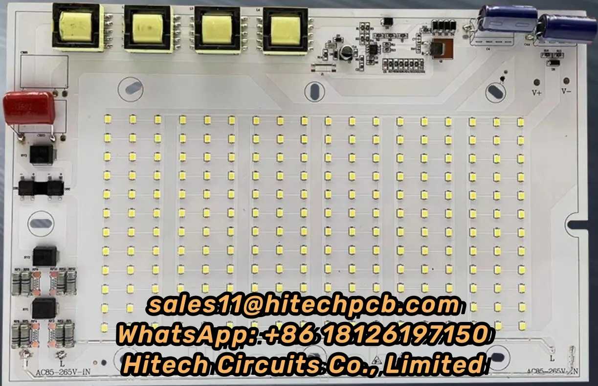
LED PCB Assembly – Hitech Circuits Co., Limited
LED PCB Assembly – Hitech Circuits Co., Limited <br> <br>What is the LED Circuit Board assembly? <br> <br>Generally, LED PCB assembly is considered to be a circuit board that has the LED components soldered to it. The LED is soldered to the printed circuit board and features a chip that creates the light as electrically connected. A thermal heat sink and a ceramic base are used to bond the chip. Not all the PCB products can be used in Led industry, as an LED PCB is easy to create a high volume of heat, but making it hard to cool with traditional methods. For this reason, metal core PCB is widely used in LED application because of their enhanced ability to dissipate heat, especially aluminum pcb is often used to fabricate PCB for LED lights. <br> <br>We’ve had great LED PCB assembly experiences with top LED chips to brand such as Cree, Luxeon, Osram, Nichia, Lumileds, MLS, EVERLIGHT, Samsung, LG, Seoul., etc. PCB LED lights can be incorporated into numerous lighting applications due to their combination of excellent energy efficiency, low cost and maximum design flexibility. <br> <br>Application of LED PCB Assembly <br> <br>Hitechpcba serves customers in different industries, providing highly reliable and innovative LED PCBs for various applications: <br> <br>• Horticulture light LED PCB Assembly <br> <br>• LED controller PCB Assembly <br> <br>• Computer LED display and indicators <br> <br>• LED lights PCB Assembly for medical use <br> <br>• Automotive LED PCBs Assembly include PCBs for brake lights and headlights <br> <br>• Street lighting LED PCB Assembly <br> <br>• Flashlights and camping accessories <br> <br>• Traffic light PCB Assembly <br> <br>• Commercial lighting LED PCB Assembly <br> <br>LED PCB Assembly specification <br> <br>Number of layers for LED PCB <br> <br>These layers are made up of aluminum and magnesium, but now have Copper base material and Ceramic base materials for LED PCB industry, we can meet it. <br> <br>Aluminum LED PCBs stand out among other PCBs because it has a good insulation characteristic and has a better machinery performance, the cheap cost is one important factor too. <br> <br>Types of layers for LED PCB Assembly <br> <br>Normally, the base layer is made using aluminum alloy metal. <br> <br>This aluminum alloy substrate used in making the base makes it ideal for through-hole technology which transfers and dissipates heat. <br> <br>A thermal insulation layer is made using some ceramic polymer which has good viscoelasticity characteristics. <br> <br>It is highly heat resistant and protects the PCB against heat and mechanical stress. <br> <br>The circuit layer, which is covered by a copper foil which can range from one to ten ounces. <br> <br> <br>LED Board type- single or in panel <br> <br>Some boards are shapeless. For this reason, LED PCB panels are used. This reduces time, labor production and testing time. <br> <br>Some LED PCB Assembly is done on a single board while others are done on panel boards. <br> <br>LED PCB Assembly Process <br> <br>Roughly, the PCBA process can be divided into theses phases: soldering paste printing > SMT (surface mounted technology) > reflow soldering > AOI (automated optical inspection)> THT (through-hole technology) > wave soldering > touch-up and cleaning > IC-programming > FCT (functional tests) > aging testing. <br> <br>Below we show you the process. <br> <br>Step1. Summarizing Project Information <br>Before contacting your supplier, make sure you have all the project information. Suppliers will need info following for quoting LED PCB assembly: <br>Gerber <br>BOM <br>LED PCB specification <br>Quotation quantity <br> <br>Once you have gathered these information, you can contact us and request for a quote. <br> <br>Of course, you can also provide the schematic, LED PCB Assembly pictures and even samples to us. The more details they have, the more accurate the supplier’s quotation will be. <br> <br>Step2. Discussion and details about custom LED PCB Assembly <br> <br>Different projects will have different requirements. Remember the special requirements mentioned in step 1? That’s going to be the focus of this session. Equipment and engineering capacity will not be identical between suppliers. Make sure your supplier has the equipment to produce and assemble major components and the corresponding testing capabilities. <br> <br>For example, some vendors don’t have X-ray testing equipment, which means they can’t check the mount quality of BGA chips. Outsourcing this step will increase risk and cost. That’s what you don’t want. <br> <br>Also, pay attention to time taken by the supplier to quote. Motherboards often contain hundreds or even thousands of components, and they are supplied by different manufacturers. To ensure the quality of the components, the supplier sourcing team will make multi-inquiries from these manufacturers or authorized suppliers to match customer’s requirement, which usually takes 2-3 business days, and even longer for some scarce chips. Therefore, if your project is complex and the supplier quotes you within few hours, double check with them. <br> <br>Step3. Sample and feedback <br>After confirming the PI, the supplier will usually provide pre-production samples for your approval. At the same time, the supplier will also confirm with you the logistics plan of the bulk goods. Make sure they understand your shipping requirements, including details on packaging, customs clearance, taxes, etc. <br> <br>For us to have a successful LED PCB Assembly process, its functions must be defined. Compliance requirement is defined to reduce the effect when components are selected. <br> <br>The Bill of Materials is then generated from the information installed on the LED PCB. <br> <br>All this information is used to assemble components which are identified from MOB to the LED PCB. <br> <br>After that, the routing of traces is determined to each component, based on the size, shape of the circuit board and location of connectors. <br> <br>Hitech Circuits is trusted by thousands of electronic engineers on their LED PCB assembly projects, from consumer, led bulb to precisely medical LED light, we can help you from the beginning of design stage; From commercial flood LED to industrial high power LED, from automotive LED to military LED, Venture is the perfect place for your LED PCB assembly requirement. <br> <br>Hitech Circuits has been participated in hundreds and thousands of LED lighting projects, by providing LED PCB and also LED PCB assembly service. <br> <br>Our LED PCB assembly had covered both ends of the Lighting Class LED size spectrum, assembling some of the largest (2 meter long boards) and some of the smallest LED Lighting applications which used in Medical Endoscopes. <br> <br>LED PCB Assembly is very crucial in the current industrial development. Many electrical devises are being innovated and the old once being improved. <br> <br>LED PCBs are useful due to the fact that they are made using materials that can transfer and dissipate heat. This characteristic increases device durability. <br> <br>The world is changing with new technology, especially PCB technology that plays an essential role in the application of LED circuits. And the LED industry is taking advantage of this technology and growing faster. <br> <br>As a full feature PCB solutions provider with more than a decade of experience, we're capable to provide LED PCB fabrication, components procurement and LED PCB assembly all under one roof. We can work with you to develop metal core PCB, aluminum circuit boards customized to your specific applications. We feature competitively priced PCBs made with standard FR-4 material that includes a thermal aluminum clad layer that will efficiently dissipate heat, keep all LED PCB components cool and significantly enhance the performance of your products. <br> <br>LED PCB Board, LED PCB Assembly <br>LED with its advantages of high brightness, high efficiency, low heat, long life, is considered the most development potential in the 21st century lighting. In the market and policy driven by the rapid development of the domestic LED industry blowout has formed a relatively complete industrial chain, including the production of epitaxial wafers, chip preparation, packaging, integration, LED application. In 2010, China's LED industry scale, up from $ 827 billion in 2019 to 220 billion yuan, an annual growth rate of over 70%, higher than the 50% level of growth of the global LED lighting industry output value. Among them, the middle and lower reaches of the most complete industrial chain, accounting for 90% of the overall percentage of the GDP. China has become the world's leading LED manufacturing base and important application market. <br> <br>To further promote the technological innovation of the LED industry, construction and wide application of independent industry chain, China Electronic Appliance Corporation and industry associations to organize the theme of "Focus on the core energy LED Exhibition will be held November 9-11, 2010 in Shanghai International Expo Center and the 78th China Electronics Fair over the same period will be held will create from raw materials, epitaxial wafers, chip, LED bracket, LED accessories, LED packaging and supporting materials, the LED backlight upstream firm to the upstream and downstream enterprises of the display, lighting, landscaping, decorative lighting, traffic lights, automotive lighting, special lighting, to the equipment, instrumentation, software, finance, consulting and other service enterprises and technological exchanges and market trading platform, help the domestic industry sustained and healthy development, and promote the steady expansion of the LED application market. <br> <br>In the LED industry chain upstream of the epitaxial wafers and LED chips accounted for 70% of the profits of the whole industry, and technology-intensive, capital-intensive, where the core technology of the LED. Well-known epitaxial wafer and chip production enterprises will be exhibited a number of energy-efficient, low heat, cost-effective LED products, many of whom have excellent products of international advanced level. <br> <br>LED electronic PCB assembly manufacturing 100% Original LED Chip with one-stop in-house PCBA services. <br> <br>For further details freely contact Cynthia at [email protected] <br>[a]https%3A%2F%2Fwww.hitechpcba.com%2Fled-pcb-assembly[/a]
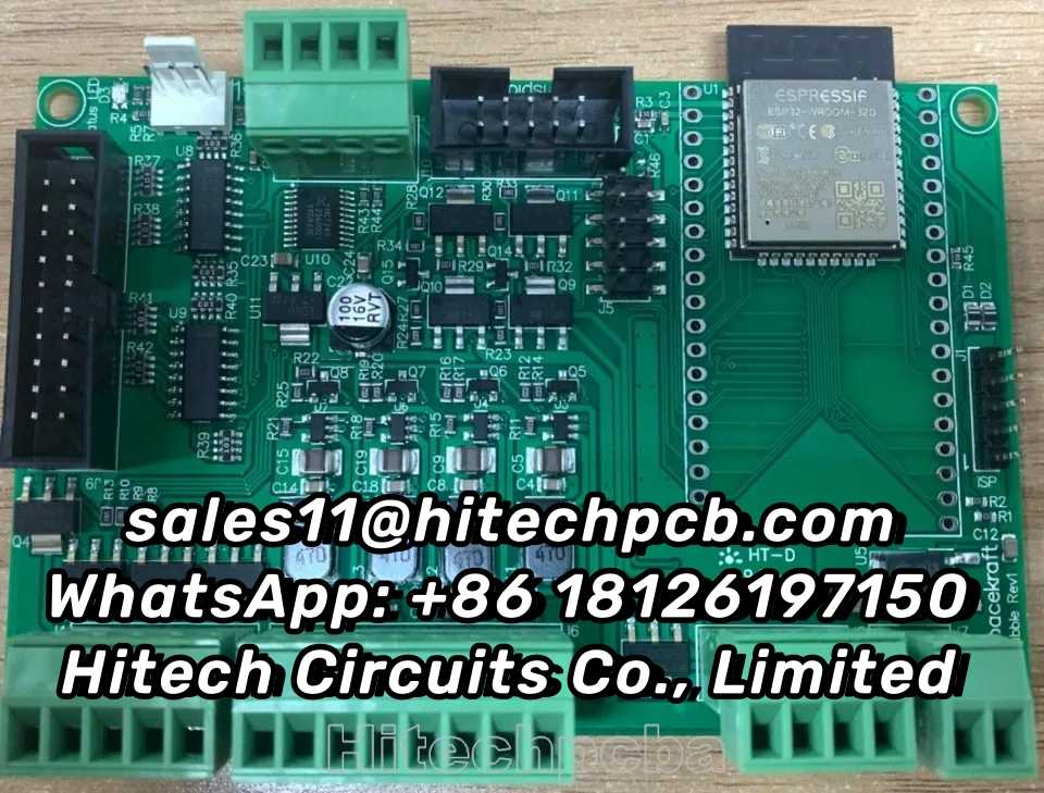
PCB Assembly Prototypes Manufacturer – Hitech Circuits Co., Limited
PCB Assembly Prototypes Manufacturer – Hitech Circuits Co., Limited <br> <br>What is a prototype PCB assembly? <br> <br> PCB prototyping is the experimentation pilot stage of the product which is to be mass produced at a later stage. This is more of an experiment which is done after the initial discussions and the design. This offers a pre-production analysis of the boards that are to be manufactured, reducing the possible number of errors in the PCB design. PCB prototypes help the manufacturer analyze the strengths as well as weak areas of their proposed circuit boards. Prototypes also serve as a reference point for future versions of the same product. At Hitechpcba, we handle PCB prototype assembly in quantities from one to hundred printed circuit boards. <br> <br> <br>We have acquired capabilities that enable us to serve our clients better. All these years, we have worked on many complex prototype PCB assembly projects, and we believe the following capabilities have helped us serve our clients better. <br> <br>Prototype PCB Assembly Services: We specialize in the following prototype printed circuit board assembly services. <br> <br>SMT: We can provide single-sided and double-sided surface mount PCB assemblies in different specifications. <br> <br>Plated Through Hole: We offer plated through hole assembly with selective soldering. <br> <br>Mixed Assemblies: We often work on projects involving mixed assemblies – through-hole and SMT and electromechanical assemblies. <br> <br>PCBA Testing: All the PCBA functional testing is performed in-house. Over the years, we have invested in various test fixtures and equipment, which helps us ensure the quality of PCBA. Currently, we provide the following types of PCBA testing services: <br> <br>Flying probe testing for PCB <br> <br>Functional testing including system and board-level testing <br> <br>General PCB Assembly Capabilities: Our general PCB assembly capabilities are not limited to these: <br> <br>RoHS, leaded or lead free, clean and no chemistries <br> <br>PCB components including various types of QFNs, BGAs, 0105, 0201, 0804, and press fit components in small quantities. <br> <br> <br>What are the benefits of a prototype PCB assembly? <br> <br>Prototype PCB assembly comes with several advantages. These benefits play a major role in the facilitation of your PCB manufacturing. Some of these benefits include: <br> <br> <br>Detection of Flaws Early <br> <br>With prototype PCB, you will easily detect whatever flaws are present during the product’s development stages. This will allow you to solve the issues thereby saving you some money if you had gone ahead to make the production having the flaws in them. <br> <br>If you go ahead to make changes during the production, there may be a need for more technicalities, and this may be expensive. <br> <br> <br>Testing of Each Component <br> <br>With a prototype, you will be able to test all your system’s elements individually before you go ahead to set it up. You should do this because it is important especially for very complex projects composed of several parts that are PCB based. <br> <br>When you validate each of these components, you will be able to identify those areas having issues that you should look into. This is the only way the project can function the right way. <br> <br> <br>Reduction in Total Costs <br> <br>Utilizing the prototype bare PCB for any of your projects could go a long way in reducing what you’ll have spent in total for the project. With prototyping, you will be able to notice those errors in your project and then make corrections before you start the real production. <br> <br>As soon as these flaws have been checked and rectified, then you may continue with the manufacturing of your Printed circuit boards in large quantities, thereby saving you unnecessary costs. <br> <br> <br>High-Quality PCBs <br> <br>Why prototyping your PCB is important is to help you test if your project will function effectively. When we talk of testing, it involves the identification of errors present and then rectifying and making corrections to them. <br> <br>Therefore, the eventual PCB after the prototyping will be of high quality that surely meets standards set internationally. <br> <br> <br>Less Turnaround Time <br> <br>With prototype PCB assembly, you will be able to reduce the total time used in producing your printed circuit board. While making use of prototype printed circuit boards, you’ll be able to see the errors and then make corrections before you start the actual production. <br> <br>Therefore, the eventual prototype will be free of defects. This implies that your PCBs will be produced quickly by your manufacturer. <br> <br> <br>What are the different types of prototype PCB assembly services you offer? <br> <br>With years of market presence and experience, we specializes in the following prototype PCB assembly services. <br> <br>Plated through-hole (PTH): We can provide the through-hole assembly with selective soldering. <br> <br>Surface mount technology (SMT): We offer single-sided as well as double-sided SMT board assemblies in varied specifications. <br> <br>Mixed Assemblies: Our experts often work on projects involving both PTH and SMT assemblies. <br> <br> <br>What are the types of testing Hitechpcba use for prototype PCB assembly? <br> <br>Automated Optical Inspection (AOI): This is performed before and after the soldering to identify the component placement, presence, and solder quality. <br> <br>X-ray Testing: In this type of testing, the operator relies on the X-ray images of the PCB to check the solder joints and lead-less components such as Quad Flat Packs and ball grid arrays, which are generally not visible to naked eyes. <br> <br>In-Circuit Testing (ICT): This method is used to detect manufacturing defects by testing the electrical properties in the SMT Assembly. <br> <br>These techniques help us ensure the reliability and accuracy of the circuit boards. In addition to this, it ensures a long operational life of equipment, minimal production losses, streamlined processes, and much more. <br> <br> <br>What are the capabilities Hitechpcba offer for prototype PCB assemblies? <br> <br>We specialize in offering IPC compliant, and quick turn PCB assemblies. We are very particular about our scheduled deliveries and timelines, and we deliver without compromising the quality. Our PCBA capabilities are not limited to these. Here are some capabilities we offer through prototype PCB assemblies. <br> <br>RoHS compliance <br> <br>Stringent testing procedures <br> <br>Device encapsulation <br> <br>Full turnkey, partial turnkey, and kitted/consigned services <br> <br>Assemblies using Surface Mount (SMT), Thru-hole, Mixed Technology (SMT/Thru-hole), Single and double-sided SMT/PTH, Large parts on both sides, BGA on both sides. <br> <br> <br>Do you perform a component analysis for prototype PCB assemblies? <br> <br>Yes, we check the quality and performance of components before mounting them on the circuit boards. This is because a malfunctioning component can affect the performance of the entire circuit board assembly and also pose risks. <br> <br> <br>What is your standard turnaround time for a prototype PCB assembly? <br> <br>Our turnaround time for standard applications is two weeks. This timeframe varies depending on the complexity of the applications. However, we are committed to offering quick turnaround times without compromising on quality, functionality, and accuracy, which offers our client a competitive advantage and reduced time to market. You can also request any emergency assistance or queries related to any type of PCB assembly. Our experts will assist you in all possible ways. <br> <br> <br>How is the cost of prototype PCB assembly estimated? <br> <br>PCBA costing varies based on the different factors, such as PCBA parts, type of materials to be used, order quantity, and much more. We can also offer quotes and customization options once you share the detailed requirement with us. <br> <br>We focus on quality and customer satisfaction over anything else. This has helped us build a long list of happy and satisfied customers. So, if you wish to partner with a manufacturer of prototype PCB assembly in China, then don’t hesitate to reach us. Our experts will assist you through all the phases of the prototype PCB assembly process. We look forward to making your experience with us better and memorable. <br> <br> <br>How to choose prototype pcb assembly manufacturer? <br> <br>Our pcb prototype assembly service includes the sourcing of components. This allows you to concentrate on what you do best: layout design. We have a dedicated sourcing staff that coordinates with multiple suppliers and distributors to purchase electronic parts as per client requirements, and our staff completes these purchasing particulars in a most efficient manner. We have advanced processes for optimal selection of packaging (cut tape, tube, bulk, etc.) to reduce the total cost. Furthermore, we are capable of cross-referencing parts and even locating hard-to-find and obsolete parts. Customers can be rest assured that when Hitech Circuits substitutes components that they are high quality: we only use the electronic component numbers and manufacturers specified in the BOM. We will not modify your original layout design. Part substitutions take place only with your permission. <br> <br>The final pcb prototype assembly service cost includes assembly labor charges, bare circuit board rates, and part costs. We understand the importance of prompt delivery. The sooner the components are sourced, the sooner we can begin circuit board fabrication. We thoroughly evaluate engineering inquiries and concerns related to the related parts with our clients before commencing circuit board assembly. The average time taken for pcb manufacturing assembly is about two weeks, which can be further reduced if there are no hard-to-locate components or documentation mistakes. <br> <br>We have specialized experts to deliver fast turnarounds for prototype circuit board assembly with surface-mount (SMT), through-hole (THT) and mixed-technology components. <br> <br>Anyone interested in electronics and electronic circuit boards needs to understand the various stages of developing and producing a printed circuit board. It can come in handy when you are seeking a top prototype smt assembly provider. The various production stages of printed circuit boards entail design, prototyping (prototype PCB development and rapid prototyping pcb assembly), and PCB high volume production. Different entities will always seek part of the whole production process depending on their electronic circuit board needs. <br> <br>However, this article seeks to help you understand everything about prototype PCB assembly, a fundamental aspect of the PCB production process. <br> <br>Rapid prototyping pcb assembly represents a fundamental phase of the printed circuit production process. It is also inferred as PCBA prototype assembly, SMT or surface-mount technology PCB prototype, PCB sample assembly, etc. From these alternative names, the meaning of prototype assembly regarding printed circuit boards becomes apparent. So what is assembly prototype? <br> <br>PCB prototype assembly service is a fast prototype printed circuit board assembly primarily used to test fresh or new electronic designs. Consequently, it assists with checking and ensuring quality assurance of the PCB. For instance, it verifies that no bug exists in the test PCB, updates the design, and finds bugs. In most instances, prototype assembly of an electronic project will require two or three iterations to ensure everything is perfect. <br> <br> <br>Why Choose Hitech Circuits PCB Assembly for Your Prototype PCB Assembly Projects? <br> <br>There are several PCB manufacturers specializing in prototype PCB assembly services. However, Hitech Circuits stands out owing to the following: <br> <br>1.Strong Supply Chain: Over the years, we have built strong supply chain relationships in the industry, which helps us fulfill the requirements of turnkey prototype assembly services easily. <br> <br>2.Fastest Turnaround Times: Our engineering expertise coupled with our understanding of industry requirements and a well-equipped facility enables us to assure the fastest turnaround times of 24-48 hours. <br> <br>3.Reliability: All the printed circuit boards that we produce are IPC compliant, which helps us assure reliability. <br> <br>4.Competitive Pricing and Quick Quote: Our supply chain relationships enable us to assure competitive prices. The cost of the PCB prototype assembly will be made available within 24-48 hours. <br> <br>For further details freely contact Cynthia at [email protected] <br>[a]https%3A%2F%2Fwww.hitechpcba.com%2Fpcb-assembly-manufacturer[/a]
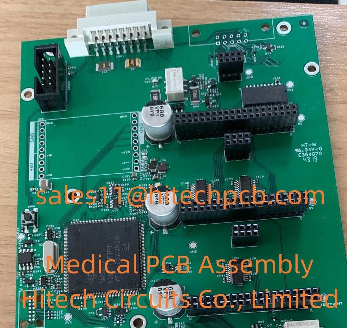
Medical PCB Assembly Manufacturer – One-stop service from Hitech Circuits Co., Limited
Medical PCB Assembly Manufacturer – One-stop service from Hitech Circuits Co., Limited <br> <br>Medical devices (medical PCB assembly) refer to instruments, devices, instruments; in vitro diagnostic reagents and calibrators, materials, and other similar or related items. There are used directly or indirectly in the human body, including the required computer software. <br> <br> <br>Hitech Circuits has extensive experience in providing medical PCB assembly services to our medical industry customers, and we deeply understand that our medical PCBA will be used in life-critical medical devices, which have extremely high requirements for precision and reliability. <br> <br>We are committed to offering the world-class PCBA by strictly controlling the quality of every piece, our medical PCB assembly, box build assembly, and prototypes assembly capacities allow us to assemble kinds of medical devices such as diagnostic imaging equipment, lasers, and handheld dental tools. <br> <br>At Hitech Circuits, we take care of the medical PCB assembly of your product so you can spend more time running your business and marketing your medical devices. <br> <br> <br> <br>Hitechpcba medical PCB assembly technique: <br> <br>Whether in a controlled environment such as a hospital or in an uncontrolled environment such as a home health care center, medical equipment must protect the lives of patients and surgeons. Medical PCBA refers to instrumented circuit boards that are used directly or indirectly in the human body. Such as instruments, equipment, instruments, in vitro diagnostic reagents, and calibrators, materials, and other similar or related instruments. <br> <br>Therefore, the requirements for component procurement and processing are very strict, and a more precise technique is required, which is produced by IPC Class 3 standard. Hitechpcba is fully certificated, apart from certifications of ISO9001:2015, ISO14001, REACH and IATF16949, we have also obtained the ISO13485 certification, which means that our PCBs can meet the high standards required by medical devices, and all of our finished medical devices are of FDA Class II. Working with us can avoid you from worrying about the quality problem. <br> <br>This standard provides you with the ability to produce and manufacture to meet higher customer needs. In the medical device industry, safety and quality are not negotiable. At every step of the product life cycle, including service and delivery, regulatory requirements are becoming more stringent. <br> <br>More and more industry organizations want to showcase their quality management processes and make sure that everything they do is best practice. PCBA is used in the medical industry to bring good news to patients. Hitechpcba is a certified manufacturer offering a one-stop PCB and PCBA turnkey service with 15 years experience and we have the confidence to become your preferred supplier. <br> <br> <br>Hitechpcba advantages: <br> <br>We offer unprecedented service and flexibility for any medical device PCB. Without a small batch test, you can’t start your concept prototype so that it doesn’t help you get it to market. We offer comprehensive engineering support to make your medical device printed circuit board manufacturing process reality in the most cost-effective way. <br> <br>We provide high-end customized processing services for PCBA in medical machinery customers. It is manufactured by PCB circuit board, component procurement, SMT chip processing, patch plug-in soldering, assembly testing and other one-stop services. <br> <br>QC was set up in front of the furnace for poor screening, PCBA 100% visual inspection after furnace, PCBA 100% optical inspection, and 13 temperature zone reflow soldering each product independently set temperature. Must undergo rigorous tests, such as ICT, FCT, Burn-in test. The products produced include monitors, pacemakers, sphygmomanometers, etc. <br> <br>We ensure the quality, reliability, and traceability of our medical PCB manufacturing assembly. <br> <br> <br> <br>Over 15 Years of Medical PCBA Experience <br> <br>With more than 10 years of experience in offering PCB assembly services, we have a good understanding of the medical industry, our experts have participated in a host of projects to provide medical PCBA solutions to leading medical companies and get trusted by them. <br> <br> <br>Types of Medical PCB Assemblies <br> <br>As a PCB expert, Hitechpcba is capable of assembling types of medical PCBs such as multi-layer PCBs, rigid, rigid-flex PCB, and flexible PCBs, and there are various PCB materials available including copper, aluminum, and standard FR4, etc. So our medical PCB assembly solutions can be used for almost all medical devices. <br> <br> <br>High Efficiency <br> <br>We utilize state-of-the-art equipment for medical PCB assembly that can reduce errors during the assembly process, meanwhile, we have proficient workers who know how to assemble PCBs correctly and efficiently. <br> <br> <br> <br>The trend of PCB Medical Industry <br> <br>The medical field is not like it used to be. Advances in technology have revolutionized the industry. This change is even more evident in electronic diagnostic, research, and treatment systems and tools. Every day, several complex electronic devices and instruments are introduced to simplify various medical procedures. This growth has largely benefited the PCBA technology industry because, without PCB in medical, new inventions would not be impossible. To meet the ever-changing needs of medical device and diagnostic machine manufacturers, today's PCB manufacturers are manufacturing extremely simple parts into highly complex PCB in medical industry. Using specialized high-speed laminates, copper and aluminum substrates, ceramics, and coatings, PCB manufacturers can make these boards best <br> <br>Custom circuit board design in medical is the trend today. The medical industry has chosen the same approach when it comes to PCB. Customers can provide the correct specifications with the full form of PCB in medical for board size in X-direction, board size in Y-direction, total number of holes, minimum alignment and pitch size in inches, board material, number of layers, surface coating, etc. Therefore, the manufacturer will work according to the given specifications and deliver the right product for your application. <br>Freely contact sales11@hitechpcb to know more details, from Cynthia <br>[a]https%3A%2F%2Fwww.hitechpcba.com%2Fmedical-pcb-assembly-manufacturer.html[/a]
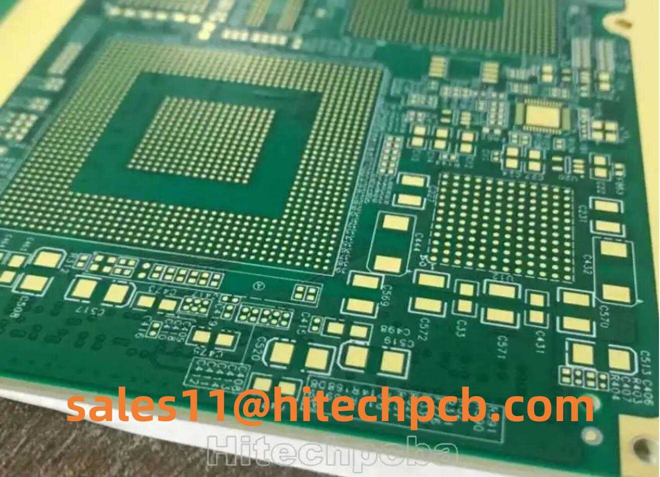
HDI PCB & High Interconnect PCB Manufacturing(from Hitech Circuits Co., Limited)
HDI PCB & High Interconnect PCB Manufacturing(from Hitech Circuits Co., Limited) <br> <br>What is a high density PCB board (HDI PCB)? <br> <br>The HDI board is based on the traditional double panel as the core board, which is made by continuously accumulating. This circuit board made by a continuous layer is also called the Build-Up Multilayer (BUM). Compared with the traditional circuit board, the HDI circuit board has the advantages of "light, thin, short, small". <br> <br>The electrical connection between HDI's plate layer is achieved by conductive pores, buried holes, and blind holes. Its structure is different from ordinary multi -layer circuit boards. A large number of blind holes are used in HDI boards. HDI PCB uses laser direct drilling, and standard PCB usually uses mechanical drilling, so the number of layers and high width ratio often decreases. <br> <br>HDI includes the use of fine features or signal traces and spaces of 0.003” (75 µm) or less and laser-drilled blind or buried microvia technology. Microvias allow the use of micro-interconnects from one layer to another within a PCB utilizing a smaller pad diameter creating additional routing density or reducing form factor. <br> <br>High-density interconnect (HDI) PCBs are characterized by finer lines, closer spaces, and more dense wiring, which allow for a faster connection while reducing the size and bulk of a project. These boards also feature blind and buried vias, laser ablated microvias, sequential lamination, and via in-pads. As a result, a HDI board can house the functionality of the previous boards used. HITECH CIRCUITS is an HDI PCB manufacturer and provider in Shenzhen, China supports HDI PCB prototype and mass production with less expensive price and quick-turn lead time. Customers from a variety of industries we serve have a common that have high expectations in quality, reliability and on-time delivery in HDI PCB production. Our quality is not afterthought, but built into each process from front-end to fabrication and shipping. <br> <br> <br>HDI PCB's advantages <br> <br>1. Reduce PCB cost: When the density of PCB increases beyond the eight-layer board, it will be manufactured in HDI, and the cost will be lower than that of traditional complicated press-forming process. <br> <br>2. Better reliability: Due to the thin thickness and the aspect ratio of 1:1, the micropores have higher reliability when transmitting signals than ordinary through holes. <br> <br>3. Improves thermal properties: The insulating dielectric material of the HDI board has a higher glass transition temperature (Tg) and therefore has better thermal properties. <br> <br>4. Improve RF interference / electromagnetic interference / electrostatic discharge (RFI / EMI ) <br> <br>5. Increase design efficiency: Micro-hole technology allows the circuit to be arranged in the inner layer, so that the circuit designer has more design space, so the efficiency of the line design can be higher. <br> <br> <br>HDI PCB Manufacturing Process <br> <br>The overall process for manufacturing HDI PCB is essentially the same as for fabricating other PCB board, with notable differences for PCB stack-up and hole drilling. Since HDI boards generally require smaller drill holes for vias, laser drilling is usually required. Although laser drills can produce smaller and more precise holes, they are limited by depth. Therefore, a limited number of layers can be drilled through at a time. For HDI boards, which are invariably multilayer and may contain buried and blind vias, multiple drilling processes may be required. This necessitates successive layer boding to achieve the desired stack-up or sequential lamination cycles. Not surprisingly, this can significantly increase PCB manufacturing time and cost. HDI PCB fabrication is an advanced technology and therefore requires expertise along with specialized equipment like laser drills, laser direct imaging (LDI) capability, and special clean room environments. In order to efficiently manufacture high-quality and reliable HDI PCB products, you must understand the HDI board manufacturing process and coordinate with your HDI PCB supplier to implement good DFM (Design for Manufacturability) for HDI layout design. Therefore, not all board factories have the ability to do the HDI, but Hitechpcb can, we will be here to support our customer needs. <br> <br> <br>-Consumer Driven Technology <br> <br>The via - in - pad process supports <br>More technology on fewer layers, proving that bigger is not always better. Since the late 1980's we have seen video cameras using cartridges the size of a novel, shrink to fit in the palm of your hand. Mobile computing and work at home have further promoted technology to make the computer faster and lighter, allowing consumers to do remote work from anywhere. <br> <br>HDI technology is the main reason for these changes. The products do more, weigh less, and their bodies are smaller. Professional equipment, mini components and thinner materials reduce the size of electronic equipment, while expanding technology, quality and speed. <br> <br> <br> <br>-Via in Pad Process <br> <br>The inspiration from the surface installation technology pushed the restrictions of BGA, COB and CSP to a smaller square surface inch. The via in pad can be placed in the surface of flat land through the cushion process. The via is plated and filled with conductive or non-conductive epoxy resin, and then close and plat it to make it almost invisible. <br> <br>It sounds simple, but there are eight steps to complete this unique process. Professional equipment and well -trained technicians followed closely to achieve perfect hiding. <br> <br> <br>-Via Fill Types <br> <br>There are many different types of via fill materials: non -conductive epoxy, epoxy, copper filling, filling and electrochemical coating. All this leads to via buried in a flat land, and the land will be fully solders as normal land. Vias and mricrovias are drilled, blind or buried, plated, and then hidden under the SMT land. Processing vias of this type of Vias requires special devices and takes time. The process time of multiple drill cycles and controlling deep drills has increased. <br> <br> <br> <br>-Cost Effective HDI <br> <br>Although the size of some consumer products is reduced, quality is still the most important factor for consumers. Use HDI technology during the design process, you can reduce the 8-layer through-hole PCB to a 4 layer HDI Microvia technology packed PCB. The elaborate HDI 4-layer PCB wiring function can achieve the same or better functions as standard 8-layer PCB. <br> <br> <br>Although the Microvia process has increased the cost of HDI PCB, the appropriate design and decrease of layers of counting reduces the cost of the ingredients of the material, and the layer count is large. <br> <br> <br>-Laser Drill Technology <br> <br>The smallest micro-vias can provide more technologies on the surface of the plate. Using a beam with a diameter of 20 microns (1 mil), this high impact can be cut through metal and glass to produce tiny via hole. There are new products, such as uniform glass materials, and they are low -loss layer pressure plates and low -dielectric constants. These materials have high heat resistance, can be used for lead -free components, and allows smaller holes. <br> <br> <br>-Lamination & Materials For HDI PCB Boards <br> <br>Advanced multilayer technology allows designers to add other layers to form a multilayer PCB. Use laser drills to produce holes in the inner layer, and can be coated when pressed, imaging and etching. The process of this increase is called sequential construction. Hitechpcb HDI PCB manufacturing uses solid -filled VIA can better heat management, connect stronger connection and improve the reliability of the board. <br> <br>The copper of the resin coating is a assistant with poor pores, with longer drilling time and thinner. Hitechpcb has ultra low contours and ultra thin copper foil, and its surface is fixed on a tiny nodule. This material has chemically treated and started chemical treatment and startup of the most fine and high quality lines and spacing technology. <br> <br>The dry resistance of the layer pressure plate still uses heating scroll method to apply resistance to core materials. It is now recommended to preheat the material to the required temperature before the layer pressure process of the HDI printing circuit board. The preheating of the material can better apply dry resistance to the surface of the layer pressure plate, pull less calories from the heat roll, and keep the stable export temperature of the layer made products consistent. The consistent entrance and exit temperature cause less air clips under the movie. This is essential for the breeding of fine lines and spacing. <br> <br> <br>-How difficult is the HDI Printed Circuits Board? <br> <br>The manufacturing of the HDI PCB (High Denity PCB) is relatively difficult because it needs to use complex manufacturing technique and technology. The following is some difficulties made by HDI PCB: <br> <br>Multi-layer plate lamination: HDI Printed Circuits Boards are usually composed of multi-layer boards, and multi-layer boards need to be laminated. Multi-layer plates need to control parameters such as temperature, time, pressure to ensure the control quality and thickness control between multi-layer boards. <br> <br>Blind holes and buried holes: HDI Printed Circuits Boards need to create blind holes and buried holes, which requires technologies such as laser drilling and chemical corrosion to ensure the accuracy and quality of the hole. <br> <br>Impedance control: HDI Printed Circuit Boards need to control impedance, which requires fine design of the layout and circuit of the circuit board, and uses special materials and processes to achieve impedance control. <br> <br>Small track space manufacturing: HDI Printed Circuits Boards need to make very small spacing tracks (conductions), which requires high-precision manufacturing equipment and technologies to ensure the accuracy and quality of the circuits. <br> <br> <br>-The difference between HDI board and normal PCB <br> <br>The HDI board is generally made of accumulation method. The more times the accumulation layer, the higher the technical grade of the board. Ordinary HDI boards are basically one accumulation. The high-end HDI uses two or more accumulated technologies, and at the same time, advanced PCB technology such as stacked holes, plating filling, and laser direct punching. When the density of PCB increases more than eight layers board, it is made by HDI, and its cost will be lower than the traditional complex compact process. <br> <br>The electrical performance and signal of the HDI board are higher than that of traditional PCB. In addition, HDI boards have improved better for radio frequency interference, electromagnetic wave interference, electrostatic release, and thermal conduction. High density integration (HDI) technology can make terminal product design more miniaturized, while meeting higher standards for electronic performance and efficiency. <br> <br>The HDI board uses a blind hole plating to perform secondary pressure, divided into one order, second order, third order, fourth, fifth order, etc. The first order is relatively simple, and the processes and processes are easy to control. The main problem of the second order is the issue of the place, and the other is the problem of punching and copper plating. There are many second order design. One is the wrong position of each order. When connecting the secondary neighborhood, it is connected to the middle layer through the wire. The method is equivalent to two first order HDI. The second is that the two order holes are overlapped. The second -order is realized by the superposition method. The processing is similar to the two first order, but there are many key points of the process. The third type is to punch perforation directly from the outer layer to the third layer (or N-2 layer). There are many different techniques from the front, and the difficulty of punching is even more difficult. <br> <br>In PCB proofing, HDI costs high, so general PCB proofing manufacturers are unwilling to do it. HITECHPCB can be a HDI Blind PCB board that others are unwilling to do. At this stage, the HDI technology adopted by HITECH has exceeded the highest number of layers of 20 layers; the number of blind holes is 1st to 4th; the minimum pore diameter is 0.076mm, and the process is laser drilling. <br> <br> <br>HDI PCB Manufacturer & Assembly – One-stop services from China <br> <br>-HDI (high-density interconnection board) is a compact circuit board designed for small capacity users. Compared with ordinary PCB, the most significant feature of HDI is that the wiring density is high. <br> <br>HDI PCB Manufacturer & Assembly – One-stop service The HDI PCB is defined as a micro via with a hole diameter of 6 mils or less and a hole diameter of 0.25 mm or less. The contact density is above 130 points/square, and the wiring density is with a line width/pitch of 3 mil/3 mil or less. HDI PCB, the full name is High Density Interconnect PCB, it requires much higher wiring density with finer trace and spacing, smaller vias and higher connection pad density. Blind and buried vias’ design is one of their marked feature. HDI PCB board is widely used in Cell phone, tablet computer, digital camera mother board PCB, GPS, Automobile board, LCD module and other different area. <br> <br>HDI PCB is the abbreviation for High Density Interconnect PCB or High Density PCB. An HDI PCB is defined as a printed circuit board with a higher wiring density per unit area than a conventional PCB. Hitech Circuits Co., Limited is a professional high density interconnect PCBs, HDI PCB board manufacturer, supplier and design company from China, if you are looking for reliable high density interconnect PCB board partner from China, please don’t hesitate to contact [email protected], from Cynthia. <br>[a]https%3A%2F%2Fwww.hitechpcba.com%2Fhdi-pcb-manufacturer-high-interconnect-pcb-manufacturing[/a]
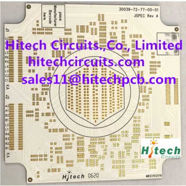
Ceramic PCB manufacturing(from Hitech Circuits Co., Limited)
Ceramic PCB manufacturing(from Hitech Circuits Co., Limited) <br> <br>Ceramic PCB have good High thermal conductivity, ceramic substrate and conductor performance, excellent chemical and thermal stability. Excellent corrosion resistance, it widely used in semiconductor,Sensor and microelectronic circuit packaging pcb, High-brightness Led chip carrier board, automotive electronics and lighting components, high-power electronic component heat dissipation materials, etc. <br> <br> <br> <br> <br>Why Purchase Your Ceramic PCBs from HITECH CIRCUITS? <br> <br>At HITECH CIRCUITS, we are dedicated to producing and selling quality PCBs to all of our customers. With over 15 years of experience in the electronic industry we are committed to producing custom ceramic PCBs that meet up with the various electronic devices at hand. <br> <br>Our professionals manufacture nothing but top-notch ceramic PCBs that are developed to tackle your demands. In addition, we assure that you will get nothing but the best and affordable prices for all the quality ceramic PCB we manufacture. Regardless of the quality of the printed circuit boards that you want, it will be gotten at a decent price. <br> <br> <br> <br>Ceramic PCB Parameter <br> <br>Ceramic PCB in high pressure, high insulation, high frequency, high temperature, and high reliable and minor volume electronic products, then Ceramic PCB will be your best choice. <br> <br>Why Ceramic PCB has such excellent performance? <br> <br>96% or 98% Alumina (Al2O3), Aluminum Nitride (ALN), or Beryllium Oxide (BeO) <br>Conductors material: For thin film technology, thick film technology, it’ll be silver palladium (AgPd), gold pllladium (AuPd); For DCB (Direct Copper Bonded) it’ll be copper only <br>Application temp: -55~850C <br>Thermal conductivity value: 16W~28W/m-K (Al2O3); 150W~240W/m-K for ALN , 220~250W/m-K for BeO; <br>Max compression strength: >7,000 N/cm2 <br>Breakdown Voltage (KV/mm): 15/20/28 for 0.25mm/0.63mm/1.0mm respectively <br>Thermal expansion conefficient(ppm/K): 7.4 (under 50~200C) <br> <br>Contact Us <br> <br>You can submit a custom request and get a price quote. <br> <br>[email protected], from Cynthia. <br>[a]https%3A%2F%2Fhitechcircuits.com%2Fproduct%2Fceramic-pcb-manufacturing%2F[/a]
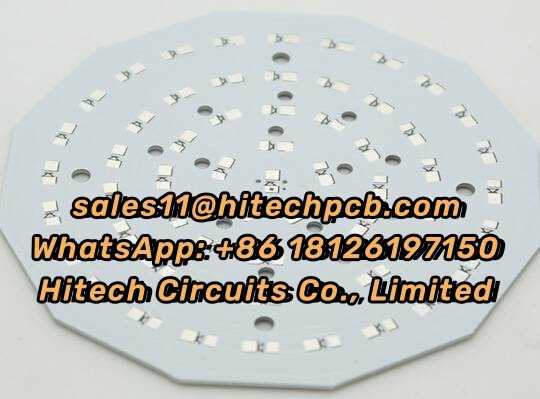
Bergquist Aluminum PCB(Hitech Circuits Co., Limited)
Bergquist Aluminum PCB(Hitech Circuits Co., Limited) <br>Bergquist Aluminum pcb board manufactured by Hitech, the Thermal Clad circuit board materials are available from The Bergquist Company in four different thermal conductivities, High Power Lighting (HPL), High Temperature (HT), Low Modulus (LM) and Multi-Purpose (MP). If you are looking are Bergquist Aluminum based pcb manufacturer in China, please contact [email protected] . <br> <br>Technical Parameters <br>Bergquist aluminum PCB <br>Base Material: Bergquist material Aluminum pcb <br>Layers: 1 <br>Thickness: 1.5mm <br>Copper thickness: 1Oz <br>plating process: Immersion gold <br>Description: LED MPCB <br>What’s Bergquist Aluminium PCB? <br>Bergquist is one of USA company, which produce Aluminium base material sheet, the performance is perfect, Aluminium base material sheet is widely used for led PCB power industry. <br> <br>Now that Power LEDs are capable of unprecedented levels of white LED brightness and luminous efficacy, they are being used in many products that are part of our daily lives. Although today the initial cost of Power LEDs is higher, many applications have demonstrated LED PCB lighting as the most cost or energy efficient solution for future installations. Bergquist provides critical thermal management support for a myriad of Power LED applications that include: medical, signage, signal, transportation, aircraft, automotive, security, portable, theatrical, commercial, residential and street lighting Power LED packaging has evolved to adapt to higher power dissipation demands. For these Power LED packages, the lowest possible thermal resistance packaging is paramount to a long and reliable service life. By combining Bergquist thermal management materials with this new and innovative packaging, progress in both light output and light quality can be achieved. <br> <br> <br>Printed Circuit Board Comparison <br> <br>Metal core PCB and standard FR-4 are commonly used circuit board materials in conjunction with Power LEDs. Bergquist’s Thermal Clad dielectric is a thin, thermally conductive layer bonded to an aluminum or copper substrate for heat dissipation (see illustration below). The key to Thermal Clad’s superior performance lies in its dielectric layer. This layer offers electrical isolation with high thermal conductivity and bonds the base metal and circuit foil together. Other manufacturers use standard prepreg as the dielectric layer, but prepreg doesn’t provide the high thermal conductivity and resulting thermal performance required to help assure the lowest possible operating temperatures and brightest light output for high-intensity LEDs PCB. Thermal Clad circuit board materials are available from The Bergquist Company in four different thermal conductivities, High Power Lighting (HPL), High Temperature (HT), Low Modulus (LM) and Multi-Purpose (MP). <br> <br>Packaging Conclusion <br> <br>Good practice suggests that you reduce the thermal resistance of that layer with Thermal Clad dielectric instead of FR-4 <br> <br>Bergquist Aluminium PCB materials types: <br> <br>Bergquist MP-06503 <br> <br>Bergquist HT04503 <br> <br>Bergquist HT07006 <br> <br>Bergquist HPL-03015 <br> <br>Bergquist HR T30.20 <br> <br>If you want to get Bergquist materials date sheet, please email to Cynthia, [email protected] <br>[a]https%3A%2F%2Fhitechcircuits.com%2Fproduct%2Fbergquist-aluminum-pcb%2F[/a]
About Cynthia_HitechPCB_manufacturing Hitech Circuits PCB's Store
No description provided.
0.0
Customer Reviews
See what others are saying about Cynthia_HitechPCB_manufacturing Hitech Circuits PCB's Store. We verify purchases to ensure reviews are genuine.
No reviews yet for this store.