

PCBAssembly _HitechCircuits's Store
Owned by PCBAssembly _HitechCircuits Joined Mar 2024 19 Listings
PCBAssembly _HitechCircuits's Store
easyid.me/biz/pcbassembly-hitechcircuits-23cc0d • Verified Store
Scan to open official EasyID digital store, view live catalog, or save business card.
Verified Merchant
EasyID Certified Seller
Fast 24h Packing
Direct courier dispatch
Zero Escrow Direct
Direct merchant settlement
Store Listings (18)
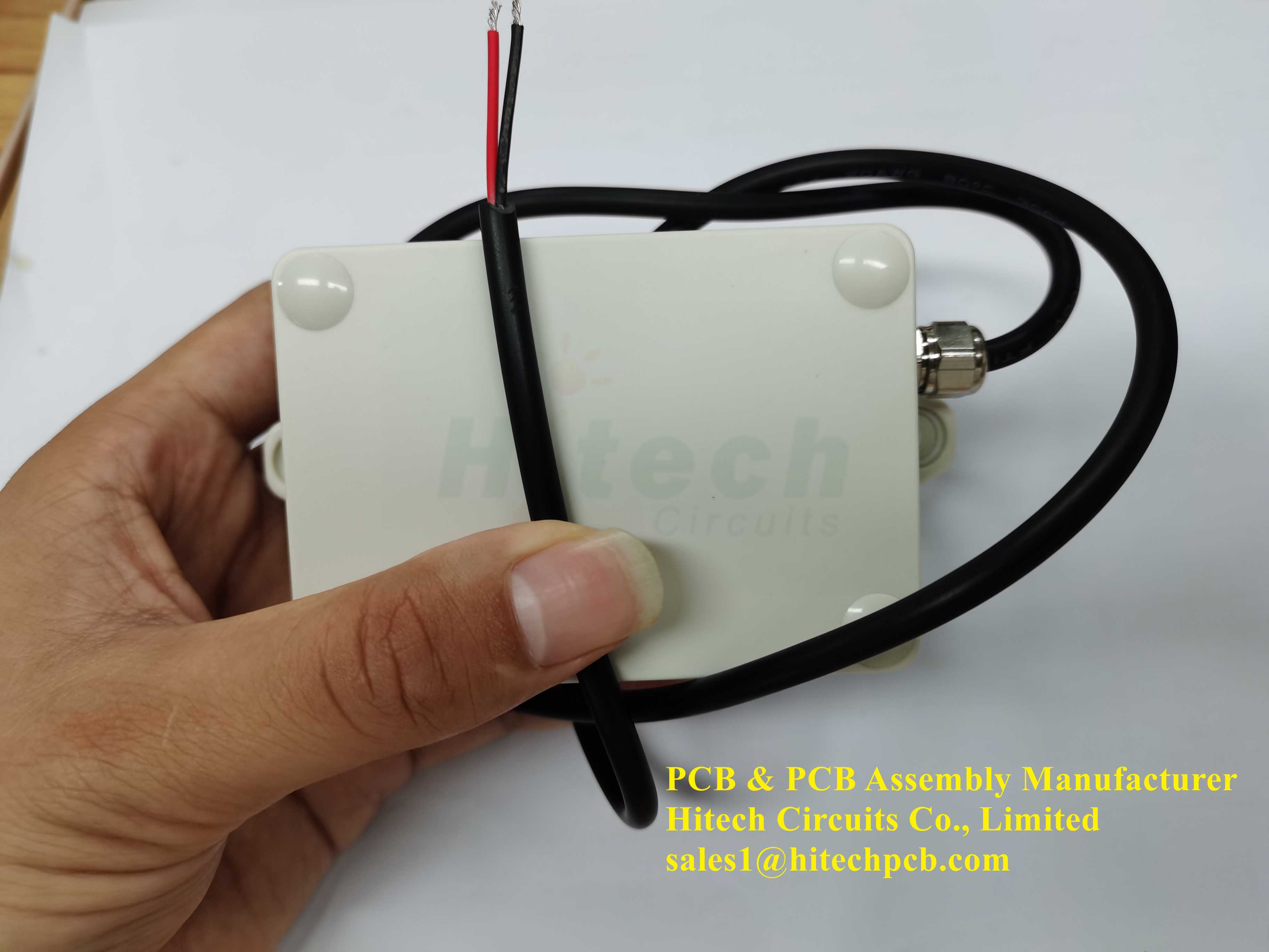
Cable & Harness Assembly by Hitech Circuits Co., Limited
Cable Assembly, also known as a wire harness, wiring harness, a cable and harness electronics, wiring assembly or wiring loom, is an assembly of electrical cables or wires which transmit signals or electrical power. Cable Assemblies are often confused with Wire Harnesses, however, the two are quite different. The main difference is that cable assemblies and harnesses normally have only two ends, whereas a wire harness contains multiple breakouts (ends) that run in many different directions with multiple terminations on each breakout.
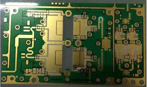
RF PCB & Microwave PCB Made by Hitech Circuits Co., Limited
What is RF PCB & Microwave PCB? <br> <br>RF PCB and microwave PCB are a type of printed circuit boards which carry the RF or microwave signal. So, these types of PCBs usually work on megahertz to gigahertz frequency ranges. Hence, we use these frequency ranges in communication technologies from mobile phones to military radars. <br> <br>The materials used are advanced composites with very specific characteristics for dielectric constant (Er), loss tangent, and CTE (co-efficient of thermal expansion). These materials can be mixed in the same Stack-Up for optimal performance and economics. <br> <br>The advantages of using materials with a low X, Y and Z CTE is a resulting PCB structure that will remain extremely stable in high temperature environments while operating at up to 40 GHz in analog applications, allowing for the effective placement of very fine pitch components including, in some cases, bare die-attach. <br> <br>RF is Radio Frequency, a signal with a very high frequency. The choice of circuit board substrate depends on the requirements for the performance indicators of the circuit board. It can be ordinary FR4 epoxy glass fiber or a special microwave substrate such as Teflon, Arlon, Rogers materials. <br> <br>As complexity of electronic components increases, the one thing that becomes imperative is signal rates and high frequency of transmission. Little surprise then that the demand for high frequency PCBs is on the rise. They find use in a variety of high-speed design applications that require a frequency range of 500MHz to 2GHz. <br> <br>[a]https%3A%2F%2Fwww.hitechpcba.com%2Frf-pcb-microwave-pcb[/a] <br>[a]https%3A%2F%2Ftwitter.com%2FRoger_PCB_PCBA[/a] <br>[a]https%3A%2F%2Fwww.facebook.com%2Fluo.roger.1675%2F[/a] <br>[a]https%3A%2F%2Fwww.instagram.com%2Froger_hitechpcb_pcba%2F[/a] <br>[a]https%3A%2F%2Fwww.hitechpcba.com[/a] <br>[a]https%3A%2F%2Fwww.hitechcircuits.com[/a] <br>[a]https%3A%2F%2Fwww.htmpcb.com[/a] <br>[email protected]
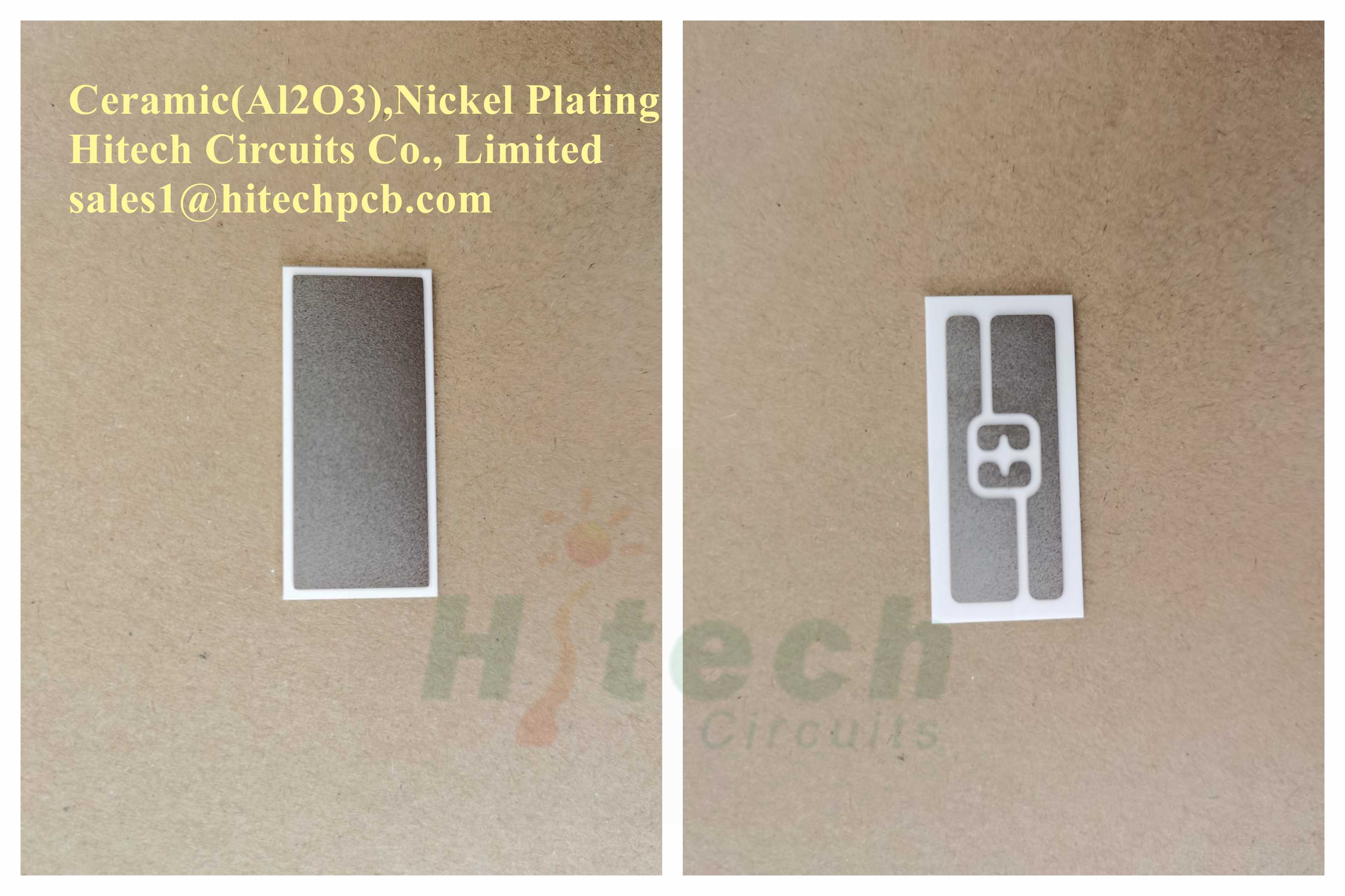
High quality Ceramic PCB board, Ceramic substrate by Hitech Circuits Co., Limited
Ceramic PCB board is also called ceramic substrate or ceramic circuit board, ceramic copper coated plate, ceramic substrate refers to the copper foil directly bonded to alumina (Al2O3) or aluminum nitride (AlN) ceramic substrate or other ceramic substrate surface (single or double) on the special process board. The ultrathin composite substrate has excellent electrical insulation performance, high thermal conductivity, excellent soft brazing and high adhesion strength, and can be etched into a variety of graphics like PCB board, with great current-carrying capacity. Therefore, Ceramic PCB board has become the basic material of high power electronic circuit structure technology and interconnection technology. <br> <br>Ceramic PCB board can do several layers at most, how many layers can be done, is a lot of customers more concerned about the topic. Ceramic PCB board can be made of multiple layers, mostly using HTCC process and LTCC process, but the processing cost is high. At present, Hitech circuit has made 4 layers, 8 layers, 16 layers of Ceramic PCB board, and so on, so far the customer feedback is good. <br> <br>[a]https%3A%2F%2Fwww.hitechpcba.com%2Fceramic-pcb[/a] <br>[a]https%3A%2F%2Ftwitter.com%2FRoger_PCB_PCBA[/a] <br>[a]https%3A%2F%2Fwww.facebook.com%2Fluo.roger.1675%2F[/a] <br>[a]https%3A%2F%2Fwww.instagram.com%2Froger_hitechpcb_pcba%2F[/a] <br>[a]https%3A%2F%2Fwww.hitechpcba.com[/a] <br>[a]https%3A%2F%2Fwww.hitechcircuits.com[/a] <br>[a]https%3A%2F%2Fwww.htmpcb.com[/a] <br>[email protected]
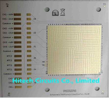
Ceramic PCB,Ceramic PCB board, Ceramic substrate or ceramic circuit board
Ceramic PCB board is also called ceramic substrate or ceramic circuit board, ceramic copper coated plate, ceramic substrate refers to the copper foil directly bonded to alumina (Al2O3) or aluminum nitride (AlN) ceramic substrate or other ceramic substrate surface (single or double) on the special process board. The ultrathin composite substrate has excellent electrical insulation performance, high thermal conductivity, excellent soft brazing and high adhesion strength, and can be etched into a variety of graphics like PCB board, with great current-carrying capacity. Therefore, Ceramic PCB board has become the basic material of high power electronic circuit structure technology and interconnection technology. <br> <br>Ceramic PCB Manufacturing & Assembly – One-stop service The ceramic substrate (ceramic PCB) refers to a special process board in which a copper foil is directly bonded to a surface of an alumina (Al2O3 ) or aluminum nitride (AlN) ceramic substrate (single or double-sided) at a high temperature. The ultra-thin composite substrate produced has excellent electrical insulation properties, high thermal conductivity, excellent solderability, and high adhesion strength, and can etch various patterns like a PCB board, and has a large current carrying current ability.
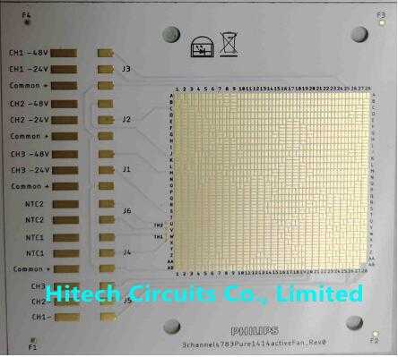
Ceramic PCB Ceramic PCB board, Ceramic substrate or ceramic circuit board
Ceramic PCB board is also called ceramic substrate or ceramic circuit board, ceramic copper coated plate, ceramic substrate refers to the copper foil directly bonded to alumina (Al2O3) or aluminum nitride (AlN) ceramic substrate or other ceramic substrate surface (single or double) on the special process board. The ultrathin composite substrate has excellent electrical insulation performance, high thermal conductivity, excellent soft brazing and high adhesion strength, and can be etched into a variety of graphics like PCB board, with great current-carrying capacity. Therefore, Ceramic PCB board has become the basic material of high power electronic circuit structure technology and interconnection technology. <br> <br>Ceramic PCB Manufacturing & Assembly – One-stop service The ceramic substrate (ceramic PCB) refers to a special process board in which a copper foil is directly bonded to a surface of an alumina (Al2O3 ) or aluminum nitride (AlN) ceramic substrate (single or double-sided) at a high temperature. The ultra-thin composite substrate produced has excellent electrical insulation properties, high thermal conductivity, excellent solderability, and high adhesion strength, and can etch various patterns like a PCB board, and has a large current carrying current ability.
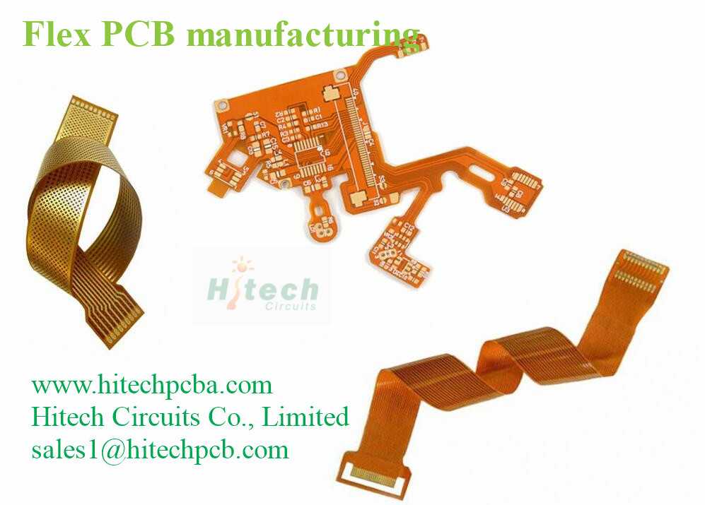
Flex PCB manufacturing
What is Flex PCB? <br> <br> <br> <br>Flexible printed circuits, also known as flex circuits, are sometimes regarded as a printed circuit board (PCB) that can bend, when in reality there are significant differences between PCB’s and flex circuits when it comes to design, fabrication and functionality. One common mistake that designers make is to design a flexible circuit using the same rules as a PCB. Flex PCB require a unique set-up and have their own set of design rules that the Hitechpcb team has termed “flex-izing” and have worked hard to perfect over the last many years. <br> <br> <br> <br>Flexible PCB, which also called Flex PCB, Flexible circuit board or flex circuit, it consists of PI base material, adhesive layer, copper layer, coverlay and sometimes with stiffeners. Flexible PCBs are now being used widely to replace traditional FR4 PCB in various different applications due to the benefits from flex PCB specially. Although more expensive than a normal rigid PCB, the right design in the right application could save weight and time in assembly, coupled with the reliability which makes flexible circuit board a worthwhile consideration. <br> <br>A flexible printed circuit consists of a metallic layer of traces, usually copper, bonded to a dielectric layer, usually polyimide. Thickness of the metal layer can be very thin (<.0001″) to very thick (> .010″) and the dielectric thickness can vary from .0005″ to .010″. Often an adhesive is used to bond the metal to the substrate, but other types of bonding such as vapor deposition can be used to attach the metal. <br> <br>Flexible PCB Manufacturing <br>What is Flex PCB? <br> <br> <br> <br>Flexible printed circuits, also known as flex circuits, are sometimes regarded as a printed circuit board (PCB) that can bend, when in reality there are significant differences between PCB’s and flex circuits when it comes to design, fabrication and functionality. One common mistake that designers make is to design a flexible circuit using the same rules as a PCB. Flex PCB require a unique set-up and have their own set of design rules that the Hitechpcb team has termed “flex-izing” and have worked hard to perfect over the last many years. <br> <br> <br> <br>Flexible PCB, which also called Flex PCB, Flexible circuit board or flex circuit, it consists of PI base material, adhesive layer, copper layer, coverlay and sometimes with stiffeners. Flexible PCBs are now being used widely to replace traditional FR4 PCB in various different applications due to the benefits from flex PCB specially. Although more expensive than a normal rigid PCB, the right design in the right application could save weight and time in assembly, coupled with the reliability which makes flexible circuit board a worthwhile consideration. <br> <br> <br> <br>A flexible printed circuit consists of a metallic layer of traces, usually copper, bonded to a dielectric layer, usually polyimide. Thickness of the metal layer can be very thin (<.0001″) to very thick (> .010″) and the dielectric thickness can vary from .0005″ to .010″. Often an adhesive is used to bond the metal to the substrate, but other types of bonding such as vapor deposition can be used to attach the metal. <br> <br>flexible PCB <br>How to calculate your flex pcb bend radius? <br> <br>Because copper tends to readily oxidize, the exposed surfaces are often covered with a protective layer, gold or solder are the two most common materials because of their conductivity and environmental durability. For non-contact areas a dielectric material is used to protect the circuitry from oxidation or electrical shorting. <br> <br>The number of material combinations that could go into a flexible printed circuit are nearly endless; current, capacitance, chemical and mechanical resistance, temperature extremes and type of flexing are just some of the criteria that impacts the material selections that best meet the functional needs. An experienced Hitechpcb design engineer takes the critical requirements into consideration when designing a circuit to meet your needs. <br> <br>Flexible printed circuit boards (FPC) has become a common component of electronic products due to its lightness and flexibility performance. It is widely used in smart terminal, wearable electronics, consumer, automotive, industrial and medical fields. The miniaturization and integrated function of electronics product development is driving FPC to fine line and multilayer design.
About PCBAssembly _HitechCircuits's Store
No description provided.
0.0
Customer Reviews
See what others are saying about PCBAssembly _HitechCircuits's Store. We verify purchases to ensure reviews are genuine.
No reviews yet for this store.