

Search results for "camera"
369 items found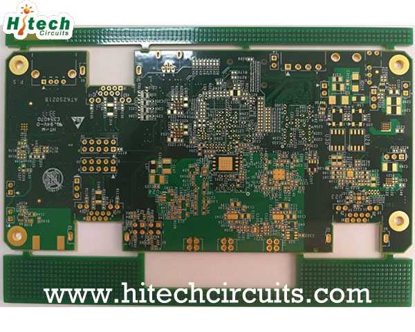
Custom rigid printed circuit board 8 layers
Rigid 8 layers printed circuit board (PCB) offers multi-layer PCB conductive wire and high density drilling, 8 layer printed circuit board is usually installed into compact devices such as digital cameras, cell phones, passive switch boxes, radios, etc; secure and reliable. Email [email protected] if you in need of multi-layer PCB. <br> <br>Website1: [a]https%3A%2F%2Fwww.hitechcircuits.com[/a] <br>Website2: [a]https%3A%2F%2Fwww.hitechpcba.com[/a] <br>Website3: [a]https%3A%2F%2Fwww.htmpcb.com[/a] <br>Email: [email protected] <br>Call/Whatsapp: +86 13302435080
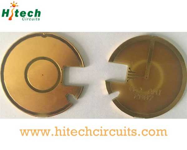
Double layers transparent PCB
The surface of the double-layer transparent pcb board is flush with the upper surface of the conductive circuit, the surface of the entire high-conductivity transparent glass-based circuit board is smooth, the conductive circuit is not easy to be damaged, and the conduction ability is strong. It is widely used in computers and peripheral auxiliary systems, medical equipment, mobile phones, digital (camera) cameras, communication equipment, precision instruments, aerospace, etc. <br> <br>Website1: [a]https%3A%2F%2Fwww.hitechcircuits.com[/a] <br>Website2: [a]https%3A%2F%2Fwww.hitechpcba.com[/a] <br>Website3: [a]https%3A%2F%2Fwww.htmpcb.com[/a] <br>Email: [email protected] <br>Call/Whatsapp: +86 13302435080

KlicPic
Klicpic is the face of hospital baby portraiture. We bring experienced, professional photographers into the hospitals to capture the baby's first photograph with a natural, artistic style. We capture this beauty by using only "real things"...natural window light, professional photographers and professional grade SLR digital cameras.
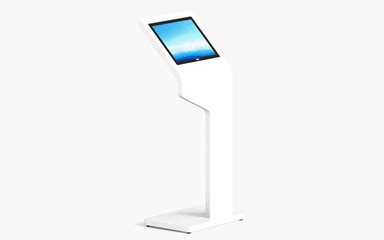
15 inch Digital Kiosk with Unique Stand
Elegant "I" design One-piece stand, commercial-grade TFT-LCD panel, 250 nits brightness, FHD resolution, clear and bright picture quality; metal body, tempered glass protective screen, sturdy and durable; exquisite and compact, simple installation, high space utilisation; optional camera, responsive capacitive touch, supports custom company logo, a fantastic add-on to your trade show booth or reception lobby area. <br> <br>We provide touch digital signage, library kiosk, kiosk system for restaurants, kiosk ordering system for restaurants, self ordering kiosk for restaurants, restaurant self service ordering kiosk, etc. For more information, please feel free to contact us! <br>#touch#digital#signage <br>[a]https%3A%2F%2Fwww.rcstarsgroup.com%2Fproducts%2F15-inch-free-standing-digital-touch-screen-kiosk-with-unique-stand%2F%0A%0A%0A%0A%0A%0A[/a]
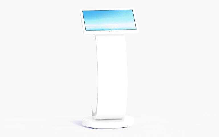
21.5 inch Interactive Digital Signage Kiosk
The unique "C"-shaped stand and round base made with superb technology, the smooth curve design makes the use environment softer; with capacitive touch, optional IR touch, 500-3500 nits brightness (default 500 nits); the metal case is sturdy and durable, available in 2E-21268 black and RC-1162 white, its screen and stand are removable; with optional camera, 4G, RFID card reader, thermal printer and other accessories, this interactive digital signage is an ideal kiosk designed for self-service and advertising display. <br> <br>Optional Panel Size: <br>21.5 inch, 32 inch <br> <br>For more information about interactive kiosks and digital board kiosk, please feel free to contact us! <br>#interactive#kiosks <br>[a]https%3A%2F%2Fwww.rcstarsgroup.com%2Fproducts%2F21.5-inch-32-inch-free-standing-touch-digital-signage-interactive-kiosks%2F%0A%0A%0A%0A[/a]
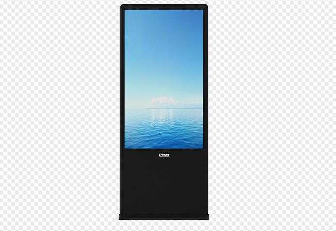
Professional Free Standing Kiosk
floor standing touch screen kiosk is designed to support connecting with media player box/PC. This free standing touch screen kiosk with built-in WiFi has New High Grade Industrial Quality and can be with design logo. By touching screens, you can see the information you need and order the things you need in the shop. This free standing touch screen kiosk is used typically to inform or advertise in public areas such as restaurants. There are major benefits for digital signs over traditional signs, including the ability to show exquisite pictures to catch clients' eyes. <br> <br>Key Features of Professional Free Standing Kiosk <br> <br>Professional free standing LCD information kiosk with a sleek and modern design that is sure to impress." The body of this type of free standing touch screen kiosk is made of high-quality metal materials and is durable. The screen resolution is up to full HD/2k/4k, and you can freely choose capacitive touch/infrared touch screen. <br> <br>The standing digital screen cover various functions that can enhance the user experience, including built-in speakers, cameras, numeric keypads, QR code scanners, RFID card readers, etc., allowing users to conduct self-service payments, self-service orders, information inquiries, processing Business etc. <br> <br>The free standing digital display screens is ideal for use in high-traffic indoor areas such as retail stores, restaurants, airports, stations, shopping malls, museums and office buildings. Because it can not only promote product/brand promotion information to users, play entertainment audio and video, public service advertisements, but also provide a series of self-service services. <br> <br>Advantages of Using Professional Free Standing Kiosk <br> <br>Improve the efficiency of information transmission: Real-time display of information through high-definition display helps people understand information more quickly and intuitively, and improves the efficiency of information transmission. <br> <br>Improve the speed of information update: Realize real-time information update through the Internet, quickly respond to information changes, and improve the speed of information update. <br> <br>Improve brand image: Through high-definition display, display corporate brand image, product information, etc. to improve brand image. <br>Improve customer experience: Improve customer experience and customer satisfaction by displaying product information, promotion information, etc. <br> <br>Save space: With vertical design, our freestanding digital signage takes up little space and is suitable for information display needs of various occasions. <br>#free#standing#lcd <br>[a]https%3A%2F%2Fwww.rcstarsgroup.com%2Fproducts%2Fprofessional-free-standing-kiosk%2F%0A%0A%0A%0A%0A%0A[/a]
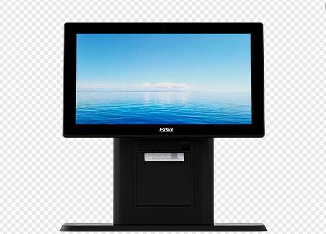
Interactive Touch Screen Table
RCSTARS interactive touchscreen tabletop digital signage is the most advanced solution for businesses and organizations to engage with their customers. With its high-quality touchscreen displays, Internet connectivity, audio and video capabilities, and durable design, this interactive touch table display is perfect for restaurants, museums, retail stores, businesses, banks, and other public spaces, offering a variety of functions such as self-service payments, inquiries, displaying information, playing audio and video, and advertising. <br> <br>Key Features of Interactive Touch Screen Table <br> <br>Elegant apearance: Highly simple and durable tablet design, choice of black or white body color, "L" type, "A" type, rotatable type, desktop stand, number of screens with 1, 2 or 3 sides, also available in silver aluminum profile. <br> <br>Robust materials: The front of the interactive table screen is covered with explosion and impact resistant tempered glass, and the back of the body is made of hardened metal for durability. <br> <br>Precise interaction: Choose fast corresponding capacitive touch/infrared touch to precisely sense each operation of you and the user. <br>Rich functions: If you want to improve the self-service terminal service based on displaying information, you can choose optional camera, printer, QR code scanner and card swiper. <br> <br>Advantages of Using interactive digital display Table <br> <br>Increase sales: Display promotional information, special offers, etc., while providing a guide to events and directing customers to place orders and spend money. <br> <br>Enhance brand image: Whether in a store or a business, the elegant look of Rcstars' interactive digital table display perfectly matches and enhances the overall atmosphere and image of the premises. <br> <br>Provide diverse services: Thanks to the multiple functions configured in the desktop interactive displays, we can simultaneously provide users with information display and inquiry, self-order and checkout, business processing, etc. At the same time, Rcstars, one of trusted and professional digital screen suppliers, also provides personalized and customized services whenever you need them. <br>#tabletop#digital#signage <br>[a]https%3A%2F%2Fwww.rcstarsgroup.com%2Fproducts%2Finteractive-touch-screen-table%2F%0A%0A%0A%0A%0A%0A[/a]

securei
Evolving Protection: Securei's Path from CCTV to Biometric Solutions <br> <br>In an era marked by technological advancements and evolving security needs, the demand for robust surveillance solutions has escalated significantly. Bangalore, a bustling metropolis known as the Silicon Valley of India, stands at the forefront of embracing cutting-edge security measures to safeguard its populace and assets. Among the pioneers in this realm is Securei, a company that commenced its journey by offering Security Camera for Commercial in Bangalore, For more :- [a]https%3A%2F%2Fmedium.com%2F%40securei%2Fevolving-protection-secureis-path-from-cctv-to-biometric-solutions-cdd94c05b80f[/a]

Wolfbox Coupon Codes & Discount
Wolfbox is a leading brand when it comes to vehicle safety products, specifically their backup cameras. These cameras are designed to give drivers a clear view of what’s behind their car <br>[a]https%3A%2F%2Fkoboon.net%2Fstores%2Fwolfbox-coupon-promo-codes%2F[/a]

Wolfbox Coupon Codes & Discount
Wolfbox is a leading brand when it comes to vehicle safety products, specifically their backup cameras. These cameras are designed to give drivers a clear view of what’s behind their car <br>[a]https%3A%2F%2Fkoboon.net%2Fstores%2Fwolfbox-coupon-promo-codes%2F[/a]
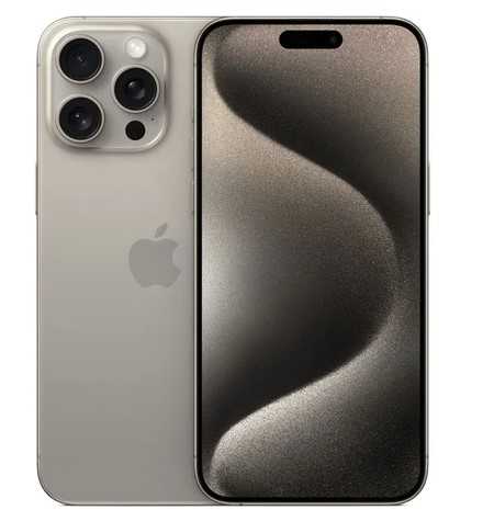
iPhone 15 Pro Max in Bangladesh
Introducing the iPhone 15 Pro Max: a pinnacle of innovation and design by Apple. This cutting-edge smartphone redefines excellence with its stunning display, lightning-fast performance, and revolutionary camera capabilities. Experience the future of mobile technology with the iPhone 15 Pro Max, available now at iStock BD for unparalleled quality and service. <br> <br>Details information now website visit. [a]https%3A%2F%2Fistockbd.com%2Fproducts%2Fiphone-15-pro-max-price-in-bd[/a]
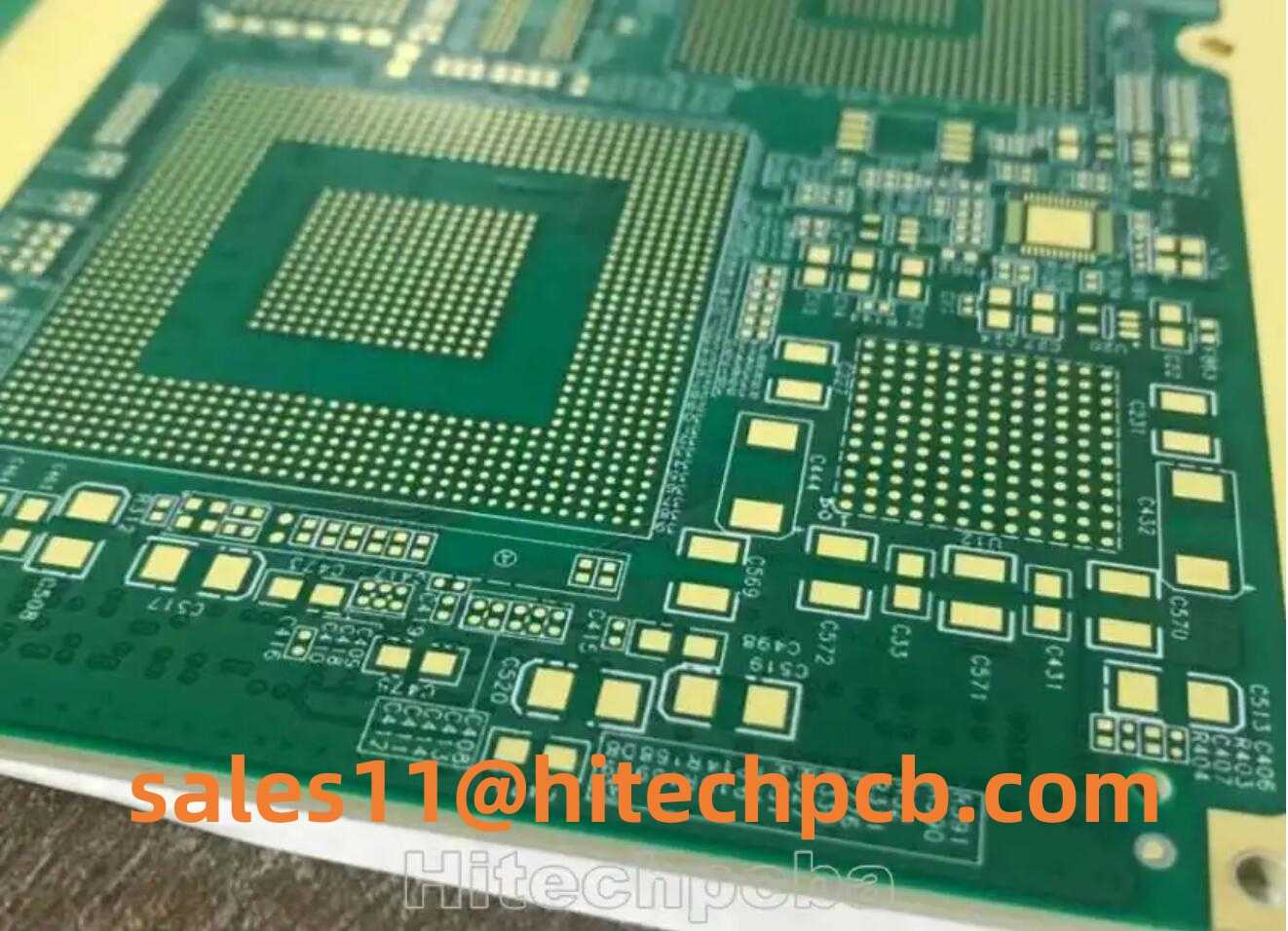
HDI PCB & High Interconnect PCB Manufacturing(from Hitech Circuits Co., Limited)
HDI PCB & High Interconnect PCB Manufacturing(from Hitech Circuits Co., Limited) <br> <br>What is a high density PCB board (HDI PCB)? <br> <br>The HDI board is based on the traditional double panel as the core board, which is made by continuously accumulating. This circuit board made by a continuous layer is also called the Build-Up Multilayer (BUM). Compared with the traditional circuit board, the HDI circuit board has the advantages of "light, thin, short, small". <br> <br>The electrical connection between HDI's plate layer is achieved by conductive pores, buried holes, and blind holes. Its structure is different from ordinary multi -layer circuit boards. A large number of blind holes are used in HDI boards. HDI PCB uses laser direct drilling, and standard PCB usually uses mechanical drilling, so the number of layers and high width ratio often decreases. <br> <br>HDI includes the use of fine features or signal traces and spaces of 0.003” (75 µm) or less and laser-drilled blind or buried microvia technology. Microvias allow the use of micro-interconnects from one layer to another within a PCB utilizing a smaller pad diameter creating additional routing density or reducing form factor. <br> <br>High-density interconnect (HDI) PCBs are characterized by finer lines, closer spaces, and more dense wiring, which allow for a faster connection while reducing the size and bulk of a project. These boards also feature blind and buried vias, laser ablated microvias, sequential lamination, and via in-pads. As a result, a HDI board can house the functionality of the previous boards used. HITECH CIRCUITS is an HDI PCB manufacturer and provider in Shenzhen, China supports HDI PCB prototype and mass production with less expensive price and quick-turn lead time. Customers from a variety of industries we serve have a common that have high expectations in quality, reliability and on-time delivery in HDI PCB production. Our quality is not afterthought, but built into each process from front-end to fabrication and shipping. <br> <br> <br>HDI PCB's advantages <br> <br>1. Reduce PCB cost: When the density of PCB increases beyond the eight-layer board, it will be manufactured in HDI, and the cost will be lower than that of traditional complicated press-forming process. <br> <br>2. Better reliability: Due to the thin thickness and the aspect ratio of 1:1, the micropores have higher reliability when transmitting signals than ordinary through holes. <br> <br>3. Improves thermal properties: The insulating dielectric material of the HDI board has a higher glass transition temperature (Tg) and therefore has better thermal properties. <br> <br>4. Improve RF interference / electromagnetic interference / electrostatic discharge (RFI / EMI ) <br> <br>5. Increase design efficiency: Micro-hole technology allows the circuit to be arranged in the inner layer, so that the circuit designer has more design space, so the efficiency of the line design can be higher. <br> <br> <br>HDI PCB Manufacturing Process <br> <br>The overall process for manufacturing HDI PCB is essentially the same as for fabricating other PCB board, with notable differences for PCB stack-up and hole drilling. Since HDI boards generally require smaller drill holes for vias, laser drilling is usually required. Although laser drills can produce smaller and more precise holes, they are limited by depth. Therefore, a limited number of layers can be drilled through at a time. For HDI boards, which are invariably multilayer and may contain buried and blind vias, multiple drilling processes may be required. This necessitates successive layer boding to achieve the desired stack-up or sequential lamination cycles. Not surprisingly, this can significantly increase PCB manufacturing time and cost. HDI PCB fabrication is an advanced technology and therefore requires expertise along with specialized equipment like laser drills, laser direct imaging (LDI) capability, and special clean room environments. In order to efficiently manufacture high-quality and reliable HDI PCB products, you must understand the HDI board manufacturing process and coordinate with your HDI PCB supplier to implement good DFM (Design for Manufacturability) for HDI layout design. Therefore, not all board factories have the ability to do the HDI, but Hitechpcb can, we will be here to support our customer needs. <br> <br> <br>-Consumer Driven Technology <br> <br>The via - in - pad process supports <br>More technology on fewer layers, proving that bigger is not always better. Since the late 1980's we have seen video cameras using cartridges the size of a novel, shrink to fit in the palm of your hand. Mobile computing and work at home have further promoted technology to make the computer faster and lighter, allowing consumers to do remote work from anywhere. <br> <br>HDI technology is the main reason for these changes. The products do more, weigh less, and their bodies are smaller. Professional equipment, mini components and thinner materials reduce the size of electronic equipment, while expanding technology, quality and speed. <br> <br> <br> <br>-Via in Pad Process <br> <br>The inspiration from the surface installation technology pushed the restrictions of BGA, COB and CSP to a smaller square surface inch. The via in pad can be placed in the surface of flat land through the cushion process. The via is plated and filled with conductive or non-conductive epoxy resin, and then close and plat it to make it almost invisible. <br> <br>It sounds simple, but there are eight steps to complete this unique process. Professional equipment and well -trained technicians followed closely to achieve perfect hiding. <br> <br> <br>-Via Fill Types <br> <br>There are many different types of via fill materials: non -conductive epoxy, epoxy, copper filling, filling and electrochemical coating. All this leads to via buried in a flat land, and the land will be fully solders as normal land. Vias and mricrovias are drilled, blind or buried, plated, and then hidden under the SMT land. Processing vias of this type of Vias requires special devices and takes time. The process time of multiple drill cycles and controlling deep drills has increased. <br> <br> <br> <br>-Cost Effective HDI <br> <br>Although the size of some consumer products is reduced, quality is still the most important factor for consumers. Use HDI technology during the design process, you can reduce the 8-layer through-hole PCB to a 4 layer HDI Microvia technology packed PCB. The elaborate HDI 4-layer PCB wiring function can achieve the same or better functions as standard 8-layer PCB. <br> <br> <br>Although the Microvia process has increased the cost of HDI PCB, the appropriate design and decrease of layers of counting reduces the cost of the ingredients of the material, and the layer count is large. <br> <br> <br>-Laser Drill Technology <br> <br>The smallest micro-vias can provide more technologies on the surface of the plate. Using a beam with a diameter of 20 microns (1 mil), this high impact can be cut through metal and glass to produce tiny via hole. There are new products, such as uniform glass materials, and they are low -loss layer pressure plates and low -dielectric constants. These materials have high heat resistance, can be used for lead -free components, and allows smaller holes. <br> <br> <br>-Lamination & Materials For HDI PCB Boards <br> <br>Advanced multilayer technology allows designers to add other layers to form a multilayer PCB. Use laser drills to produce holes in the inner layer, and can be coated when pressed, imaging and etching. The process of this increase is called sequential construction. Hitechpcb HDI PCB manufacturing uses solid -filled VIA can better heat management, connect stronger connection and improve the reliability of the board. <br> <br>The copper of the resin coating is a assistant with poor pores, with longer drilling time and thinner. Hitechpcb has ultra low contours and ultra thin copper foil, and its surface is fixed on a tiny nodule. This material has chemically treated and started chemical treatment and startup of the most fine and high quality lines and spacing technology. <br> <br>The dry resistance of the layer pressure plate still uses heating scroll method to apply resistance to core materials. It is now recommended to preheat the material to the required temperature before the layer pressure process of the HDI printing circuit board. The preheating of the material can better apply dry resistance to the surface of the layer pressure plate, pull less calories from the heat roll, and keep the stable export temperature of the layer made products consistent. The consistent entrance and exit temperature cause less air clips under the movie. This is essential for the breeding of fine lines and spacing. <br> <br> <br>-How difficult is the HDI Printed Circuits Board? <br> <br>The manufacturing of the HDI PCB (High Denity PCB) is relatively difficult because it needs to use complex manufacturing technique and technology. The following is some difficulties made by HDI PCB: <br> <br>Multi-layer plate lamination: HDI Printed Circuits Boards are usually composed of multi-layer boards, and multi-layer boards need to be laminated. Multi-layer plates need to control parameters such as temperature, time, pressure to ensure the control quality and thickness control between multi-layer boards. <br> <br>Blind holes and buried holes: HDI Printed Circuits Boards need to create blind holes and buried holes, which requires technologies such as laser drilling and chemical corrosion to ensure the accuracy and quality of the hole. <br> <br>Impedance control: HDI Printed Circuit Boards need to control impedance, which requires fine design of the layout and circuit of the circuit board, and uses special materials and processes to achieve impedance control. <br> <br>Small track space manufacturing: HDI Printed Circuits Boards need to make very small spacing tracks (conductions), which requires high-precision manufacturing equipment and technologies to ensure the accuracy and quality of the circuits. <br> <br> <br>-The difference between HDI board and normal PCB <br> <br>The HDI board is generally made of accumulation method. The more times the accumulation layer, the higher the technical grade of the board. Ordinary HDI boards are basically one accumulation. The high-end HDI uses two or more accumulated technologies, and at the same time, advanced PCB technology such as stacked holes, plating filling, and laser direct punching. When the density of PCB increases more than eight layers board, it is made by HDI, and its cost will be lower than the traditional complex compact process. <br> <br>The electrical performance and signal of the HDI board are higher than that of traditional PCB. In addition, HDI boards have improved better for radio frequency interference, electromagnetic wave interference, electrostatic release, and thermal conduction. High density integration (HDI) technology can make terminal product design more miniaturized, while meeting higher standards for electronic performance and efficiency. <br> <br>The HDI board uses a blind hole plating to perform secondary pressure, divided into one order, second order, third order, fourth, fifth order, etc. The first order is relatively simple, and the processes and processes are easy to control. The main problem of the second order is the issue of the place, and the other is the problem of punching and copper plating. There are many second order design. One is the wrong position of each order. When connecting the secondary neighborhood, it is connected to the middle layer through the wire. The method is equivalent to two first order HDI. The second is that the two order holes are overlapped. The second -order is realized by the superposition method. The processing is similar to the two first order, but there are many key points of the process. The third type is to punch perforation directly from the outer layer to the third layer (or N-2 layer). There are many different techniques from the front, and the difficulty of punching is even more difficult. <br> <br>In PCB proofing, HDI costs high, so general PCB proofing manufacturers are unwilling to do it. HITECHPCB can be a HDI Blind PCB board that others are unwilling to do. At this stage, the HDI technology adopted by HITECH has exceeded the highest number of layers of 20 layers; the number of blind holes is 1st to 4th; the minimum pore diameter is 0.076mm, and the process is laser drilling. <br> <br> <br>HDI PCB Manufacturer & Assembly – One-stop services from China <br> <br>-HDI (high-density interconnection board) is a compact circuit board designed for small capacity users. Compared with ordinary PCB, the most significant feature of HDI is that the wiring density is high. <br> <br>HDI PCB Manufacturer & Assembly – One-stop service The HDI PCB is defined as a micro via with a hole diameter of 6 mils or less and a hole diameter of 0.25 mm or less. The contact density is above 130 points/square, and the wiring density is with a line width/pitch of 3 mil/3 mil or less. HDI PCB, the full name is High Density Interconnect PCB, it requires much higher wiring density with finer trace and spacing, smaller vias and higher connection pad density. Blind and buried vias’ design is one of their marked feature. HDI PCB board is widely used in Cell phone, tablet computer, digital camera mother board PCB, GPS, Automobile board, LCD module and other different area. <br> <br>HDI PCB is the abbreviation for High Density Interconnect PCB or High Density PCB. An HDI PCB is defined as a printed circuit board with a higher wiring density per unit area than a conventional PCB. Hitech Circuits Co., Limited is a professional high density interconnect PCBs, HDI PCB board manufacturer, supplier and design company from China, if you are looking for reliable high density interconnect PCB board partner from China, please don’t hesitate to contact [email protected], from Cynthia. <br>[a]https%3A%2F%2Fwww.hitechpcba.com%2Fhdi-pcb-manufacturer-high-interconnect-pcb-manufacturing[/a]
Custom rigid printed circuit board 8 layers
Rigid 8 layers printed circuit board (PCB) offers multi-layer PCB conductive wire and high density drilling, 8 layer printed circuit board is usually installed into compact devices such as digital cameras, cell phones, passive switch boxes, radios, etc; secure and reliable. Email [email protected] if you in need of multi-layer PCB. <br> <br>Website1: [a]https%3A%2F%2Fwww.hitechcircuits.com[/a] <br>Website2: [a]https%3A%2F%2Fwww.hitechpcba.com[/a] <br>Website3: [a]https%3A%2F%2Fwww.htmpcb.com[/a] <br>Email: [email protected] <br>Call/Whatsapp: +86 13302435080
Double layers transparent PCB
The surface of the double-layer transparent pcb board is flush with the upper surface of the conductive circuit, the surface of the entire high-conductivity transparent glass-based circuit board is smooth, the conductive circuit is not easy to be damaged, and the conduction ability is strong. It is widely used in computers and peripheral auxiliary systems, medical equipment, mobile phones, digital (camera) cameras, communication equipment, precision instruments, aerospace, etc. <br> <br>Website1: [a]https%3A%2F%2Fwww.hitechcircuits.com[/a] <br>Website2: [a]https%3A%2F%2Fwww.hitechpcba.com[/a] <br>Website3: [a]https%3A%2F%2Fwww.htmpcb.com[/a] <br>Email: [email protected] <br>Call/Whatsapp: +86 13302435080
KlicPic
Klicpic is the face of hospital baby portraiture. We bring experienced, professional photographers into the hospitals to capture the baby's first photograph with a natural, artistic style. We capture this beauty by using only "real things"...natural window light, professional photographers and professional grade SLR digital cameras.
15 inch Digital Kiosk with Unique Stand
Elegant "I" design One-piece stand, commercial-grade TFT-LCD panel, 250 nits brightness, FHD resolution, clear and bright picture quality; metal body, tempered glass protective screen, sturdy and durable; exquisite and compact, simple installation, high space utilisation; optional camera, responsive capacitive touch, supports custom company logo, a fantastic add-on to your trade show booth or reception lobby area. <br> <br>We provide touch digital signage, library kiosk, kiosk system for restaurants, kiosk ordering system for restaurants, self ordering kiosk for restaurants, restaurant self service ordering kiosk, etc. For more information, please feel free to contact us! <br>#touch#digital#signage <br>[a]https%3A%2F%2Fwww.rcstarsgroup.com%2Fproducts%2F15-inch-free-standing-digital-touch-screen-kiosk-with-unique-stand%2F%0A%0A%0A%0A%0A%0A[/a]
21.5 inch Interactive Digital Signage Kiosk
The unique "C"-shaped stand and round base made with superb technology, the smooth curve design makes the use environment softer; with capacitive touch, optional IR touch, 500-3500 nits brightness (default 500 nits); the metal case is sturdy and durable, available in 2E-21268 black and RC-1162 white, its screen and stand are removable; with optional camera, 4G, RFID card reader, thermal printer and other accessories, this interactive digital signage is an ideal kiosk designed for self-service and advertising display. <br> <br>Optional Panel Size: <br>21.5 inch, 32 inch <br> <br>For more information about interactive kiosks and digital board kiosk, please feel free to contact us! <br>#interactive#kiosks <br>[a]https%3A%2F%2Fwww.rcstarsgroup.com%2Fproducts%2F21.5-inch-32-inch-free-standing-touch-digital-signage-interactive-kiosks%2F%0A%0A%0A%0A[/a]
Professional Free Standing Kiosk
floor standing touch screen kiosk is designed to support connecting with media player box/PC. This free standing touch screen kiosk with built-in WiFi has New High Grade Industrial Quality and can be with design logo. By touching screens, you can see the information you need and order the things you need in the shop. This free standing touch screen kiosk is used typically to inform or advertise in public areas such as restaurants. There are major benefits for digital signs over traditional signs, including the ability to show exquisite pictures to catch clients' eyes. <br> <br>Key Features of Professional Free Standing Kiosk <br> <br>Professional free standing LCD information kiosk with a sleek and modern design that is sure to impress." The body of this type of free standing touch screen kiosk is made of high-quality metal materials and is durable. The screen resolution is up to full HD/2k/4k, and you can freely choose capacitive touch/infrared touch screen. <br> <br>The standing digital screen cover various functions that can enhance the user experience, including built-in speakers, cameras, numeric keypads, QR code scanners, RFID card readers, etc., allowing users to conduct self-service payments, self-service orders, information inquiries, processing Business etc. <br> <br>The free standing digital display screens is ideal for use in high-traffic indoor areas such as retail stores, restaurants, airports, stations, shopping malls, museums and office buildings. Because it can not only promote product/brand promotion information to users, play entertainment audio and video, public service advertisements, but also provide a series of self-service services. <br> <br>Advantages of Using Professional Free Standing Kiosk <br> <br>Improve the efficiency of information transmission: Real-time display of information through high-definition display helps people understand information more quickly and intuitively, and improves the efficiency of information transmission. <br> <br>Improve the speed of information update: Realize real-time information update through the Internet, quickly respond to information changes, and improve the speed of information update. <br> <br>Improve brand image: Through high-definition display, display corporate brand image, product information, etc. to improve brand image. <br>Improve customer experience: Improve customer experience and customer satisfaction by displaying product information, promotion information, etc. <br> <br>Save space: With vertical design, our freestanding digital signage takes up little space and is suitable for information display needs of various occasions. <br>#free#standing#lcd <br>[a]https%3A%2F%2Fwww.rcstarsgroup.com%2Fproducts%2Fprofessional-free-standing-kiosk%2F%0A%0A%0A%0A%0A%0A[/a]
Interactive Touch Screen Table
RCSTARS interactive touchscreen tabletop digital signage is the most advanced solution for businesses and organizations to engage with their customers. With its high-quality touchscreen displays, Internet connectivity, audio and video capabilities, and durable design, this interactive touch table display is perfect for restaurants, museums, retail stores, businesses, banks, and other public spaces, offering a variety of functions such as self-service payments, inquiries, displaying information, playing audio and video, and advertising. <br> <br>Key Features of Interactive Touch Screen Table <br> <br>Elegant apearance: Highly simple and durable tablet design, choice of black or white body color, "L" type, "A" type, rotatable type, desktop stand, number of screens with 1, 2 or 3 sides, also available in silver aluminum profile. <br> <br>Robust materials: The front of the interactive table screen is covered with explosion and impact resistant tempered glass, and the back of the body is made of hardened metal for durability. <br> <br>Precise interaction: Choose fast corresponding capacitive touch/infrared touch to precisely sense each operation of you and the user. <br>Rich functions: If you want to improve the self-service terminal service based on displaying information, you can choose optional camera, printer, QR code scanner and card swiper. <br> <br>Advantages of Using interactive digital display Table <br> <br>Increase sales: Display promotional information, special offers, etc., while providing a guide to events and directing customers to place orders and spend money. <br> <br>Enhance brand image: Whether in a store or a business, the elegant look of Rcstars' interactive digital table display perfectly matches and enhances the overall atmosphere and image of the premises. <br> <br>Provide diverse services: Thanks to the multiple functions configured in the desktop interactive displays, we can simultaneously provide users with information display and inquiry, self-order and checkout, business processing, etc. At the same time, Rcstars, one of trusted and professional digital screen suppliers, also provides personalized and customized services whenever you need them. <br>#tabletop#digital#signage <br>[a]https%3A%2F%2Fwww.rcstarsgroup.com%2Fproducts%2Finteractive-touch-screen-table%2F%0A%0A%0A%0A%0A%0A[/a]
securei
Evolving Protection: Securei's Path from CCTV to Biometric Solutions <br> <br>In an era marked by technological advancements and evolving security needs, the demand for robust surveillance solutions has escalated significantly. Bangalore, a bustling metropolis known as the Silicon Valley of India, stands at the forefront of embracing cutting-edge security measures to safeguard its populace and assets. Among the pioneers in this realm is Securei, a company that commenced its journey by offering Security Camera for Commercial in Bangalore, For more :- [a]https%3A%2F%2Fmedium.com%2F%40securei%2Fevolving-protection-secureis-path-from-cctv-to-biometric-solutions-cdd94c05b80f[/a]
Wolfbox Coupon Codes & Discount
Wolfbox is a leading brand when it comes to vehicle safety products, specifically their backup cameras. These cameras are designed to give drivers a clear view of what’s behind their car <br>[a]https%3A%2F%2Fkoboon.net%2Fstores%2Fwolfbox-coupon-promo-codes%2F[/a]
Wolfbox Coupon Codes & Discount
Wolfbox is a leading brand when it comes to vehicle safety products, specifically their backup cameras. These cameras are designed to give drivers a clear view of what’s behind their car <br>[a]https%3A%2F%2Fkoboon.net%2Fstores%2Fwolfbox-coupon-promo-codes%2F[/a]
iPhone 15 Pro Max in Bangladesh
Introducing the iPhone 15 Pro Max: a pinnacle of innovation and design by Apple. This cutting-edge smartphone redefines excellence with its stunning display, lightning-fast performance, and revolutionary camera capabilities. Experience the future of mobile technology with the iPhone 15 Pro Max, available now at iStock BD for unparalleled quality and service. <br> <br>Details information now website visit. [a]https%3A%2F%2Fistockbd.com%2Fproducts%2Fiphone-15-pro-max-price-in-bd[/a]
HDI PCB & High Interconnect PCB Manufacturing(from Hitech Circuits Co., Limited)
HDI PCB & High Interconnect PCB Manufacturing(from Hitech Circuits Co., Limited) <br> <br>What is a high density PCB board (HDI PCB)? <br> <br>The HDI board is based on the traditional double panel as the core board, which is made by continuously accumulating. This circuit board made by a continuous layer is also called the Build-Up Multilayer (BUM). Compared with the traditional circuit board, the HDI circuit board has the advantages of "light, thin, short, small". <br> <br>The electrical connection between HDI's plate layer is achieved by conductive pores, buried holes, and blind holes. Its structure is different from ordinary multi -layer circuit boards. A large number of blind holes are used in HDI boards. HDI PCB uses laser direct drilling, and standard PCB usually uses mechanical drilling, so the number of layers and high width ratio often decreases. <br> <br>HDI includes the use of fine features or signal traces and spaces of 0.003” (75 µm) or less and laser-drilled blind or buried microvia technology. Microvias allow the use of micro-interconnects from one layer to another within a PCB utilizing a smaller pad diameter creating additional routing density or reducing form factor. <br> <br>High-density interconnect (HDI) PCBs are characterized by finer lines, closer spaces, and more dense wiring, which allow for a faster connection while reducing the size and bulk of a project. These boards also feature blind and buried vias, laser ablated microvias, sequential lamination, and via in-pads. As a result, a HDI board can house the functionality of the previous boards used. HITECH CIRCUITS is an HDI PCB manufacturer and provider in Shenzhen, China supports HDI PCB prototype and mass production with less expensive price and quick-turn lead time. Customers from a variety of industries we serve have a common that have high expectations in quality, reliability and on-time delivery in HDI PCB production. Our quality is not afterthought, but built into each process from front-end to fabrication and shipping. <br> <br> <br>HDI PCB's advantages <br> <br>1. Reduce PCB cost: When the density of PCB increases beyond the eight-layer board, it will be manufactured in HDI, and the cost will be lower than that of traditional complicated press-forming process. <br> <br>2. Better reliability: Due to the thin thickness and the aspect ratio of 1:1, the micropores have higher reliability when transmitting signals than ordinary through holes. <br> <br>3. Improves thermal properties: The insulating dielectric material of the HDI board has a higher glass transition temperature (Tg) and therefore has better thermal properties. <br> <br>4. Improve RF interference / electromagnetic interference / electrostatic discharge (RFI / EMI ) <br> <br>5. Increase design efficiency: Micro-hole technology allows the circuit to be arranged in the inner layer, so that the circuit designer has more design space, so the efficiency of the line design can be higher. <br> <br> <br>HDI PCB Manufacturing Process <br> <br>The overall process for manufacturing HDI PCB is essentially the same as for fabricating other PCB board, with notable differences for PCB stack-up and hole drilling. Since HDI boards generally require smaller drill holes for vias, laser drilling is usually required. Although laser drills can produce smaller and more precise holes, they are limited by depth. Therefore, a limited number of layers can be drilled through at a time. For HDI boards, which are invariably multilayer and may contain buried and blind vias, multiple drilling processes may be required. This necessitates successive layer boding to achieve the desired stack-up or sequential lamination cycles. Not surprisingly, this can significantly increase PCB manufacturing time and cost. HDI PCB fabrication is an advanced technology and therefore requires expertise along with specialized equipment like laser drills, laser direct imaging (LDI) capability, and special clean room environments. In order to efficiently manufacture high-quality and reliable HDI PCB products, you must understand the HDI board manufacturing process and coordinate with your HDI PCB supplier to implement good DFM (Design for Manufacturability) for HDI layout design. Therefore, not all board factories have the ability to do the HDI, but Hitechpcb can, we will be here to support our customer needs. <br> <br> <br>-Consumer Driven Technology <br> <br>The via - in - pad process supports <br>More technology on fewer layers, proving that bigger is not always better. Since the late 1980's we have seen video cameras using cartridges the size of a novel, shrink to fit in the palm of your hand. Mobile computing and work at home have further promoted technology to make the computer faster and lighter, allowing consumers to do remote work from anywhere. <br> <br>HDI technology is the main reason for these changes. The products do more, weigh less, and their bodies are smaller. Professional equipment, mini components and thinner materials reduce the size of electronic equipment, while expanding technology, quality and speed. <br> <br> <br> <br>-Via in Pad Process <br> <br>The inspiration from the surface installation technology pushed the restrictions of BGA, COB and CSP to a smaller square surface inch. The via in pad can be placed in the surface of flat land through the cushion process. The via is plated and filled with conductive or non-conductive epoxy resin, and then close and plat it to make it almost invisible. <br> <br>It sounds simple, but there are eight steps to complete this unique process. Professional equipment and well -trained technicians followed closely to achieve perfect hiding. <br> <br> <br>-Via Fill Types <br> <br>There are many different types of via fill materials: non -conductive epoxy, epoxy, copper filling, filling and electrochemical coating. All this leads to via buried in a flat land, and the land will be fully solders as normal land. Vias and mricrovias are drilled, blind or buried, plated, and then hidden under the SMT land. Processing vias of this type of Vias requires special devices and takes time. The process time of multiple drill cycles and controlling deep drills has increased. <br> <br> <br> <br>-Cost Effective HDI <br> <br>Although the size of some consumer products is reduced, quality is still the most important factor for consumers. Use HDI technology during the design process, you can reduce the 8-layer through-hole PCB to a 4 layer HDI Microvia technology packed PCB. The elaborate HDI 4-layer PCB wiring function can achieve the same or better functions as standard 8-layer PCB. <br> <br> <br>Although the Microvia process has increased the cost of HDI PCB, the appropriate design and decrease of layers of counting reduces the cost of the ingredients of the material, and the layer count is large. <br> <br> <br>-Laser Drill Technology <br> <br>The smallest micro-vias can provide more technologies on the surface of the plate. Using a beam with a diameter of 20 microns (1 mil), this high impact can be cut through metal and glass to produce tiny via hole. There are new products, such as uniform glass materials, and they are low -loss layer pressure plates and low -dielectric constants. These materials have high heat resistance, can be used for lead -free components, and allows smaller holes. <br> <br> <br>-Lamination & Materials For HDI PCB Boards <br> <br>Advanced multilayer technology allows designers to add other layers to form a multilayer PCB. Use laser drills to produce holes in the inner layer, and can be coated when pressed, imaging and etching. The process of this increase is called sequential construction. Hitechpcb HDI PCB manufacturing uses solid -filled VIA can better heat management, connect stronger connection and improve the reliability of the board. <br> <br>The copper of the resin coating is a assistant with poor pores, with longer drilling time and thinner. Hitechpcb has ultra low contours and ultra thin copper foil, and its surface is fixed on a tiny nodule. This material has chemically treated and started chemical treatment and startup of the most fine and high quality lines and spacing technology. <br> <br>The dry resistance of the layer pressure plate still uses heating scroll method to apply resistance to core materials. It is now recommended to preheat the material to the required temperature before the layer pressure process of the HDI printing circuit board. The preheating of the material can better apply dry resistance to the surface of the layer pressure plate, pull less calories from the heat roll, and keep the stable export temperature of the layer made products consistent. The consistent entrance and exit temperature cause less air clips under the movie. This is essential for the breeding of fine lines and spacing. <br> <br> <br>-How difficult is the HDI Printed Circuits Board? <br> <br>The manufacturing of the HDI PCB (High Denity PCB) is relatively difficult because it needs to use complex manufacturing technique and technology. The following is some difficulties made by HDI PCB: <br> <br>Multi-layer plate lamination: HDI Printed Circuits Boards are usually composed of multi-layer boards, and multi-layer boards need to be laminated. Multi-layer plates need to control parameters such as temperature, time, pressure to ensure the control quality and thickness control between multi-layer boards. <br> <br>Blind holes and buried holes: HDI Printed Circuits Boards need to create blind holes and buried holes, which requires technologies such as laser drilling and chemical corrosion to ensure the accuracy and quality of the hole. <br> <br>Impedance control: HDI Printed Circuit Boards need to control impedance, which requires fine design of the layout and circuit of the circuit board, and uses special materials and processes to achieve impedance control. <br> <br>Small track space manufacturing: HDI Printed Circuits Boards need to make very small spacing tracks (conductions), which requires high-precision manufacturing equipment and technologies to ensure the accuracy and quality of the circuits. <br> <br> <br>-The difference between HDI board and normal PCB <br> <br>The HDI board is generally made of accumulation method. The more times the accumulation layer, the higher the technical grade of the board. Ordinary HDI boards are basically one accumulation. The high-end HDI uses two or more accumulated technologies, and at the same time, advanced PCB technology such as stacked holes, plating filling, and laser direct punching. When the density of PCB increases more than eight layers board, it is made by HDI, and its cost will be lower than the traditional complex compact process. <br> <br>The electrical performance and signal of the HDI board are higher than that of traditional PCB. In addition, HDI boards have improved better for radio frequency interference, electromagnetic wave interference, electrostatic release, and thermal conduction. High density integration (HDI) technology can make terminal product design more miniaturized, while meeting higher standards for electronic performance and efficiency. <br> <br>The HDI board uses a blind hole plating to perform secondary pressure, divided into one order, second order, third order, fourth, fifth order, etc. The first order is relatively simple, and the processes and processes are easy to control. The main problem of the second order is the issue of the place, and the other is the problem of punching and copper plating. There are many second order design. One is the wrong position of each order. When connecting the secondary neighborhood, it is connected to the middle layer through the wire. The method is equivalent to two first order HDI. The second is that the two order holes are overlapped. The second -order is realized by the superposition method. The processing is similar to the two first order, but there are many key points of the process. The third type is to punch perforation directly from the outer layer to the third layer (or N-2 layer). There are many different techniques from the front, and the difficulty of punching is even more difficult. <br> <br>In PCB proofing, HDI costs high, so general PCB proofing manufacturers are unwilling to do it. HITECHPCB can be a HDI Blind PCB board that others are unwilling to do. At this stage, the HDI technology adopted by HITECH has exceeded the highest number of layers of 20 layers; the number of blind holes is 1st to 4th; the minimum pore diameter is 0.076mm, and the process is laser drilling. <br> <br> <br>HDI PCB Manufacturer & Assembly – One-stop services from China <br> <br>-HDI (high-density interconnection board) is a compact circuit board designed for small capacity users. Compared with ordinary PCB, the most significant feature of HDI is that the wiring density is high. <br> <br>HDI PCB Manufacturer & Assembly – One-stop service The HDI PCB is defined as a micro via with a hole diameter of 6 mils or less and a hole diameter of 0.25 mm or less. The contact density is above 130 points/square, and the wiring density is with a line width/pitch of 3 mil/3 mil or less. HDI PCB, the full name is High Density Interconnect PCB, it requires much higher wiring density with finer trace and spacing, smaller vias and higher connection pad density. Blind and buried vias’ design is one of their marked feature. HDI PCB board is widely used in Cell phone, tablet computer, digital camera mother board PCB, GPS, Automobile board, LCD module and other different area. <br> <br>HDI PCB is the abbreviation for High Density Interconnect PCB or High Density PCB. An HDI PCB is defined as a printed circuit board with a higher wiring density per unit area than a conventional PCB. Hitech Circuits Co., Limited is a professional high density interconnect PCBs, HDI PCB board manufacturer, supplier and design company from China, if you are looking for reliable high density interconnect PCB board partner from China, please don’t hesitate to contact [email protected], from Cynthia. <br>[a]https%3A%2F%2Fwww.hitechpcba.com%2Fhdi-pcb-manufacturer-high-interconnect-pcb-manufacturing[/a]