

Search results for "camera"
369 items found
Tools and Equipment
In the automotive industry, numerous tools and equipment are used for various purposes, including repair, maintenance, and manufacturing. Here are some of the commonly used tools and equipment: <br>1. Hand tools: <br> - Wrenches (open-end, box-end, combination, ratcheting), Sockets and ratchets, Screwdrivers (flat-head, Phillips, Torx, etc.), Pliers (slip-joint, locking, needle-nose, etc.), Hammers (ball-peen, dead-blow, rubber mallet), Pry bars and trim removal tools, Wire strippers and crimpers <br>2. Power tools: <br> - Impact wrenches (air or electric), Drills (corded or cordless), Grinders (angle grinders, die grinders), Saws (reciprocating, circular, jigsaw), Pneumatic tools (air ratchets, air hammers, air chisels) <br>3. Diagnostic tools: <br> - Scan tools (OBD-II scanners, code readers), Multimeters, Circuit testers, Compression testers, Vacuum gauges, Timing lights, Borescopes and inspection cameras <br>4. Lifting and jacking equipment: <br> - Floor jacks, Jack stands, Hydraulic lifts (two-post, four-post, in-ground), Engine hoists and cherry pickers <br>5. Specialty tools: <br> - Pullers (bearing, gear, etc.), Brake tools (caliper compressors, brake bleeders), Torque wrenches, Locking pliers (Vise-Grips), Wheel alignment equipment, Tire changers and balancers <br>6. Lubrication and fluid transfer equipment: <br> - Grease guns, Oil drain pans, Fluid transfer pumps, Funnels and pour spouts <br>7. Shop equipment: <br> - Workbenches and tool chests, Parts washers, Air compressors, Welding equipment, Hydraulic presses <br>These tools and equipment are essential for professionals working in automotive repair shops, dealerships, and manufacturing facilities to perform their tasks efficiently and safely.
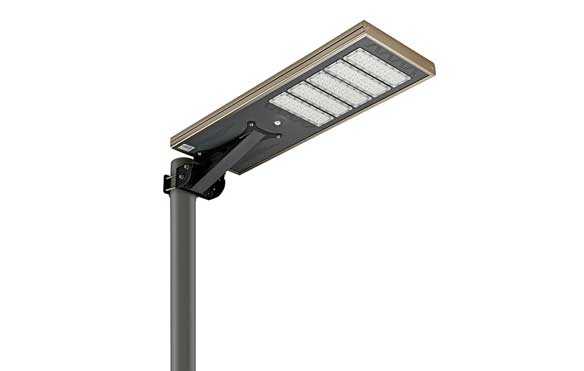
SOLAR LIGHT FOR FARM
[a]https%3A%2F%2Fwww.css-solar.com%2Fsolar-light-for-farm.html[/a] <br> <br>Outdoor solar powered farm lights are mainly used in farms, industrial parks, main traffic intersections, and other areas. <br> <br>Normally, solar lights for farmhouse will be equipped with a monitoring function, which can monitor the situation in a certain range in real-time according to the needs of customers. <br> <br>And now solar-powered farm lights are basically high-definition monitoring cameras, with WiFi + 4G function. Under any condition, a solar light for farm is recorded within the range. In some large farms, manors, and industrial parks, you can often spot solar powered lights wholesale for farmhouses. <br> <br>Outdoor solar farm lights not only provide lighting needs but also meet the monitoring and recording needs of most customers. The solar power system is also available, which saves a lot of expenses for many farmers, such as cable laying and pipe laying. <br> <br>Solar Light For Farm Advantages <br>Outdoor solar farm lights, also known as solar-powered farm lights, offer several advantages over traditional lighting systems. Here are some of the key benefits of using solar-powered lights on farms: <br> <br>Cost savings: One of the most significant advantages of using outdoor solar farm lights is the cost savings. Since they are powered by the sun, they don't require electricity from the grid, which can be expensive. This means that you can significantly reduce your electricity bills and save money in the long run.

Security installation in canberra and brisbane
Newhams: Security installers in Brisbane are professionals who specialize in the installation, maintenance, and servicing of security systems for residential, commercial, and industrial properties in the Brisbane area. These systems can include CCTV cameras, alarm systems, access control systems, intercoms, and monitoring services. <br> <br>Security installers in Brisbane typically offer a range of services tailored to the specific needs of their clients. This can include: <br> <br>Consultation and Assessment: They assess the security needs of a property and provide recommendations on the most suitable security solutions based on factors such as location, property layout, and budget. <br> <br>Installation: They install security systems efficiently and effectively, ensuring that all components are properly configured and integrated for optimal performance. <br> <br>Maintenance and Servicing: They offer regular maintenance services to ensure that security systems are functioning correctly and are up to date with the latest technology and security standards. This can include system checks, software updates, and hardware replacements as needed. <br> <br>24/7 Monitoring: Many security installers in Brisbane offer 24/7 monitoring services, where security professionals monitor the property remotely for any signs of unauthorized activity or security breaches. In the event of an alarm trigger, they can quickly respond and dispatch appropriate authorities if necessary. <br> <br>Customer Support: They provide ongoing customer support to address any questions or concerns that clients may have regarding their security systems. This can include troubleshooting, training on system usage, and assistance with system upgrades or expansions. <br> <br>Overall, security installers in Brisbane play a crucial role in helping individuals and businesses protect their properties and assets against various security threats, providing peace of mind and ensuring a safe and secure environment.

Best Makeup Artist in Jaipur
Looking for the epitome of beauty transformations in Jaipur? Look no further than the best makeup artist in Jaipur! With a skillful touch and an eye for detail, they weave magic with brushes and palettes, turning ordinary into extraordinary. Whether it's for a special occasion or a photoshoot, their expertise promises to accentuate your natural beauty and leave you feeling like royalty. From flawless foundation to mesmerizing eye looks, they craft personalized creations that make heads turn and cameras click. With their artistry, your vision of stunning makeup becomes a radiant reality in the vibrant city of Jaipur.
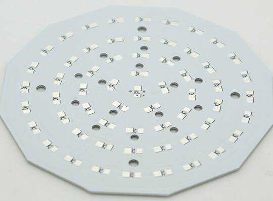
Aluminum PCB & Metal Core PCB & LED PCB Circuit board
Aluminium PCB are metal-based, copper-clad laminates with a good heat dissipation function. Usually, Aluminium PCB is refer to LED PCB board, which is the most important part of LED display and lighting products, etc. <br> <br>Hitech Circuits Co., Limited is a professional aluminum pcb board, LED PCB manufacturer in China. Through 10 years of aluminum pcb board designing and manufacturing experience, Hitech are able to provide high quality and cost effective single layer, double layer and multi layer aluminum pcb boards to global customers. For any of your requirements regarding aluminum pcb board, please don’t hesitate to contact [email protected] . <br> <br>What is aluminium PCB board ? <br>Aluminium PCB board, also named Aluminium based PCB, metal clad (MCPCB) PCB, insulated metal substrate(IMS or IMPCB) PCB, thermally conductive PCBs, etc. Aluminum printed circuit board ( PCB ) is a unique metal-based copper clad laminate with good thermal conductivity, electrical insulation performance and mechanical processing performance. It is composed of copper foil, thermally conductive insulating layer and metal substrate. It is generally including single layer, double layer and multi layer aluminum pcb board. <br> <br>The structure of aluminum printed circuit boards <br>Generally speaking, the PCB aluminum substrate is composed of a circuit layer, a thermally conductive insulating layer and a metal base layer; it can be divided into three layers: <br> <br>Circuit layer: equivalent to the copper clad laminate of an ordinary PCB, the thickness of the circuit copper foil is 1 to 10 oz. The circuit layer (that is, copper foil) is usually etched to form a printed circuit to connect the various components of the assembly. Generally, the circuit layer requires a large current-carrying capacity, so thicker copper foil should be used, with a thickness of 35μm~ 280μm; <br> <br>Insulation layer: The insulation layer is a layer of low thermal resistance thermally conductive insulating material. The thickness is 0.003 to 0.006 inches. It is generally composed of a special polymer filled with special ceramics. It has low thermal resistance, excellent viscoelasticity, thermal aging resistance, and can withstand mechanical and thermal stress. It is the core technology of aluminum-based copper clad laminates. Our aluminum printed circuit boards have obtained UL certification. <br> <br>Metal base layer: The metal base layer is the support member of the aluminium pcb, which requires high thermal conductivity, generally aluminum plate will be used, copper plate can also be used (copper plate can provide better thermal conductivity), suitable for conventional machinery such as drilling, punching and cutting processing. <br> <br>Main usages and applications of aluminium PCB board: <br>Audio devices: input, output amplifiers, balanced amplifiers, audio amplifier, preamplifier, power amplifier etc. <br>Power Supply: switching regulator, DC / AC converter, SW regulator . <br>Telecommunications electronic equipment: high-frequency electric amplifiers, filtering appliance, transmitter circuit etc . <br>Office automation equipment: electric motor, drivers etc . <br>Automotive: electronic regulator, ignition, power controllers etc . <br>Computer: CPU board, floppy drive, power device etc . <br>Power Modules: converter, solid-state relay, power rectifier bridges etc . <br>Lamps Lighting: with the promotion of energy-saving lamps, Aluminum base PCB , are widely used on LED lights. <br>Aluminum pcb vs fr4 pcb board <br>FR4 board is a code name for the grade of flame-retardant material. It represents a material specification that the resin material must be able to extinguish by itself after burning. It is not a material name, but a material grade. Therefore, there are many types of FR-4 grade materials used for pcb, but most of them are composite materials made of so-called Tera-Function epoxy resin, Filler and glass fiber. <br> <br>FR-4 PCB board, according to different uses, industry insider generally call them: FR-4 Epoxy Glass Cloth, insulating board, epoxy board, epoxy resin board, brominated epoxy resin board, FR-4 , Fiberglass board, fiberglass board, FR-4 reinforcement board, FPC reinforcement board, flexible circuit board reinforcement board, FR-4 epoxy resin board, flame-retardant insulation board, FR-4 laminated board, epoxy board , FR-4 light board, FR-4 fiberglass board, epoxy glass cloth board, epoxy glass cloth laminate, circuit board drilling pad etc. <br> <br>Main technical features and applications of FR-4 board: stable electrical insulation performance, good flatness, smooth surface, no pits, thickness tolerance standards, suitable for high-performance electronic insulation requirements products, such as FPC reinforcement board, PCB drilling pad, glass fiber meson, potentiometer carbon film printed glass fiber board, precision star gear (wafer grinding), precision test plate, electrical (electrical) equipment insulation support spacer, insulation backing plate, transformer insulation plate, motor insulation, grinding gear, electronic switch insulation board, etc. <br> <br>The aluminum pcb board is a metal-based copper-clad laminate with good heat dissipation function. Generally, a single-sided aluminum PCB is composed of a three-layer structure, which is a circuit layer (copper foil), an insulating layer and a metal base layer. For high-end use, it is also designed as a double-sided board, and the structure is circuit layer, insulating layer, aluminum base, insulating layer, and circuit layer. Very few applications are multi-layer boards, which can be formed by bonding ordinary multi-layer boards with insulating layers and aluminum bases. <br> <br>Compared with traditional FR-4 PCB, aluminum pcb circuit boards have the following advantages: <br> <br>Good thermal conductivity. The metal layer of the aluminum pcb board can quickly dissipate heat, transfer the heat of the device, minimize the thermal resistance, and have good thermal conductivity. <br>More environmentally friendly. Aluminum-based pcb boards do not contain substances harmful to human health and the environment, and are more environmentally friendly than FR-4 circuit boards. <br>High durability. FR-4 pcb may be warped, bent, cracked etc during production and transportation; ceramic substrates are also more fragile. Aluminum pcb circuit boards make up for the shortcomings of FR-4 boards and ceramic substrates, have longer durability, and avoid board cracks caused by production and transportation. <br>Higher performance. The circuit layer of the aluminum-based PCB board is etched to form the circuit. Compared with the traditional FR-4 pcb board, under the same line width, thickness, etc., the current carried by the aluminum pcb is higher than that of the FR-4 pcb board. <br>Features of aluminum material that used to manufacturing Aluminium PCB Board <br>Regarding Aluminum PCB or wrote as Aluminium PCB, there are different types of Aluminum which used for the laminate of Aluminium base pcb, the brief introduction as below. <br> <br>There are mainly three different types of metal aluminum base that commonly used, including 1000 series, 5000 series and 6000 series, the basic features of these three series aluminum base are as follows: <br> <br>(1) 1050, 1060, 1070 are the typical types of 1000 series, 1000 series is also known as pure aluminum base, which is the purest of all the series, the purity can reach more than 99.00%. Because this series do not contain other technical elements, so the production process is single and simple, the price is relatively cheap as well, It is currently the most commonly used series in conventional industry. nowadays, 1050 and 1060 are most widely used in the market. 1000 series aluminium base determine the range of the minimum aluminium content according to the last two digits, such as series 1050 , the last two digits are 50, according to the international brand naming principles, its aluminum content must be more than 99.5%, it is unqualified if less than 99.5%. Our country standard (GB/T3880-2006) is clearly stipulated in 1050 must reached 99.5% aluminum content. Same as 1060 series that aluminum content must be above 99.6%. <br> <br>(2) 5000 series include 5052, 5005, 5083, 5A05 series. 5000 series belongs to alloy aluminum base series which is commonly used, the main elements is magnesium, about 3-5% magnesium element, so it is also known as aluminum and magnesium alloys. The main features are low density, high tensile strength and high elongation rate. Under the same area, the weight of the aluminum magnesium alloy is lower than other series, so is the reason why often used in aviation, such as aircraft fuel tank. In other conventional industries are widely used as well. The processing technology belongs to the series of hot rolled aluminum base, therefore can do oxidation processing. At present, 5052 is the most widely used in 5000 series. <br> <br>(3) 6061 belongs to 6000 series, which mainly contains magnesium and silicon two kinds of elements. 6061 is a kind of cold treatment of aluminium products, applicable to against corrosion, oxidation demanding. The general characteristics of 6061: excellent interface characteristics, easy to coating, high strength, good workability, strong corrosion resistance. 6061 aluminum base typical applications: aircraft parts, camera parts, coupler, ship accessories and metal, electronic components and connectors, etc. <br> <br>Advantages of aluminum PCB printed circuit boards <br>It is more suitable for SMT process; <br>Meet the requirements of RoHs; <br>The heat dissipation has been effectively treated, thereby reducing the operating temperature of the module, prolonging the service life and improving the reliability; <br>The volume is decreasing, reducing the assembly area of radiators and other hardware, reducing product volume, and reducing hardware and assembly costs; <br>Good mechanical durability, better than ceramic circuit boards made by some simple processes. <br>Disadvantages of aluminum pcb printed circuit boards <br>Higher cost: Compared with other cheap PCB products, the price of aluminum-based PCB boards accounts for 30% of the total product price. <br>At present, the mainstream manufacturer can only make single-sided PCB boards, and it is difficult to make double-sided aluminum PCB boards. At present, single-sided aluminum PCB boards are relatively skilled in China, and the process and technology of multi-layer aluminum PCB boards are relatively mature in foreign countries. Good news is, through years of aluminum pcb board designing and manufacturing, Hitech are able to provide high quality and cost effective single layer, double layer and multi layer aluminum pcb boards. <br>The thermal conductivity test method and the test result do not match, the thermal conductivity of the dielectric layer and the thermal conductivity of the aluminum-based PCB board are different to a certain extent. <br>The material standards for aluminum-based copper-clad PCB boards are not unified. There are CPCA industry standards, national standards, international standards, etc. <br>If the thickness of the copper foil does not meet the standard, it will cause some phenomena such as burning the circuit and exploding the power supply. However, we never occur such problems. <br>Does HiTech Circuits offer technical support for designing Aluminum PCBs? <br>Yes, HiTech Circuits provides comprehensive technical support, including design assistance and recommendations to optimize your PCB for manufacturing efficiency and performance.
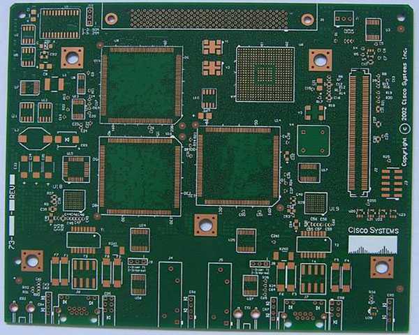
High Density Interconnect PCB from Hitech Circuits
HDI pcb is the abbreviation for High Density Interconnect pcb or High Density pcb. An HDI PCB is defined as a printed circuit board with a higher wiring density per unit area than a conventional PCB. Hitech Circuits Co., Limited is a professional high density interconnect pcbs, hdi pcb board manufacturer, supplier and design company from China, if you are looking for reliable high density interconnect PCb board partner from China, please don’t hesitate to contact [email protected] . <br>What is a high-density interconnection PCB board <br>HDI is the abbreviation of High Density Interconnection, which is a kind of technology for the production of printed circuit boards. High density interconnection PCB board is a circuit board with a relatively high line distribution density using micro-blind and buried via technology. <br> <br>HDI includes the use of fine features or signal traces and spaces of 0.003” (75 µm) or less and laser-drilled blind or buried microvia technology. Microvias allow the use of micro-interconnects from one layer to another within a PCB utilizing a smaller pad diameter creating additional routing density or reducing form factor. <br> <br>HDI pcb board is a compact product designed for small-capacity users. <br> <br>Advantages of high-density interconnected PCB boards <br>It can reduce the cost of PCB: When the density of PCB increases to more than eight-layer board, it is manufactured by HDI, and its cost will be lower than that of the traditional complex pressing process. <br>Increase circuit density: has better interconnection than that of traditional circuit boards and parts <br>Conducive to the use of advanced construction technology <br>Have better electrical performance and signal accuracy <br>Better reliability <br>Can improve thermal properties <br>It can improve radio frequency interference ( RFI ), electromagnetic wave interference ( EMI ), electrostatic discharge ( ESD ) <br>Increase design efficiency <br>Disadvantages of high-density interconnected PCB boards <br>The value of NDI impedance focuses on pattern transfer (complexity of patterns) and pattern electroplating process. <br>The quantity and quality are abnormal, especially the high-density circuit part of the HDI PCB board has a slower etch rate than the isolation line, which causes the isolation line to be over-etched. <br>When the entire HDI board is etched after electroplating, a large area of copper on the PCB circuit board will be etched away, which increases the production cost. At the same time, a large amount of copper ions enter the waste liquid after etching, causing environmental pollution and difficulty in recycling. <br>High-density interconnection PCB board Vs ordinary PCB board <br>Ordinary PCB board is mainly FR-4, which is laminated with epoxy resin and electronic grade glass cloth. Generally, traditional HDI PCB board uses backed copper foil on the outer surface, because laser drilling cannot penetrate the glass cloth, glass fiber-free backed copper foil is generally used. However, the current high-energy laser drilling machine can penetrate 1180 glass cloth. This is no difference from ordinary PCB board materials. <br> <br>Applications of high-density interconnected PCB boards <br>While electronic design is constantly improving the performance of the whole equipment, researchers are also working hard to reduce its size. In small portable products ranging from mobile phones to smart weapons, “small” is an eternal pursuit. High-density interconnection (HDI PCB) technology can make terminal product designs more compact, while meeting higher standards of electronic performance and efficiency. HDI PCB board is widely used in mobile phones, digital cameras, MP3, MP4, notebook computers, automotive electronics, IC carrier boards and other digital products, among which mobile phones are the most widely used. <br> <br>High density PCB is used extensively in applications and industries including <br> <br>Cell phone <br>GPS <br>Telecom <br>Semiconductor <br>Automotive <br>Military <br>Medical <br>Instrumentation <br>Note book computers <br>IC Carrier board <br>Healthcare <br>FAQs for Hitech Circuits on HDI PCBs <br>1. What types of HDI PCBs are available at Hitech Circuits? <br>Hitech Circuits offers a range of HDI PCBs, including those with through vias from surface to surface, with buried vias and through vias, sequential lamination with various materials, and with passive substrate constructions having no electrical connection. Each type caters to specific design and performance requirements. <br> <br>2. Can Hitech Circuits accommodate custom HDI PCB designs? <br>Absolutely! Hitech Circuits specializes in custom HDI PCB designs tailored to meet unique project requirements. Our team works closely with clients to understand their needs and deliver high-quality, precise PCBs that fit their specifications. <br> <br>3. What materials are used in the manufacturing of HDI PCBs? <br>HDI PCBs at Hi-Tech Circuits are made from various high-quality materials, including FR-4, high-frequency materials (such as Rogers and Taconic), and flex and rigid-flex materials. Material selection depends on the application’s requirements, such as thermal management, electrical performance, and mechanical durability. <br> <br>4. How does Hitech Circuits ensure the quality of their HDI PCBs? <br>Quality assurance is paramount at Hitech Circuits. We employ stringent quality control processes at every manufacturing stage, from design and material selection to fabrication and testing. Our HDI PCBs undergo multiple quality checks, including electrical testing, visual inspection, and automated optical inspection (AOI) to ensure they meet the highest standards. <br> <br>5. What are the lead times for HDI PCB production? <br>Lead times for HDI PCB production can vary based on the complexity of the design and the quantity required. Generally, prototype orders can be completed within a few days to two weeks, while larger production orders may take several weeks. We strive to meet our clients’ deadlines and can provide more specific timeframes upon order placement. <br> <br>6. Are there any design guidelines for HDI PCBs I should follow? <br>Yes, Hitech Circuits provides detailed design guidelines for HDI PCBs, which include recommendations on trace width, spacing, via sizes, and layer stacking. These guidelines help ensure the manufacturability of your design and optimize performance. Our team is also available to assist with any design questions. <br> <br>7. Can Hitech Circuits support high-volume HDI PCB orders? <br>Certainly! Hitech Circuits is equipped to handle high-volume orders with the same attention to detail and quality assurance as smaller orders. We have the capacity and expertise to meet the demands of large-scale production runs efficiently. <br> <br>8. How can I get a quote for my HDI PCB project? <br>Getting a quote is easy! Visit our website, and fill out the quote request form with your project details, such as PCB specifications, quantity, and any special requirements. Our sales team will review your information and provide you with a detailed quote promptly.

Private Investigator Calabasas
Nestled in the picturesque hills of Los Angeles County, Calabasas is a vibrant community known for its affluent neighborhoods, celebrity residents, and upscale amenities. However, like any other place, Calabasas is not immune to various challenges and mysteries that may require professional investigation. Private investigators in Calabasas play a crucial role in uncovering truths, resolving disputes, and providing valuable insights to clients. Let's delve into the world of private investigation in Calabasas. <br> <br>1. Comprehensive Investigative Services <br>Private investigators in Calabasas offer a wide range of investigative services tailored to meet the diverse needs of their clients: <br> <br>Surveillance: Using advanced surveillance techniques and technology, investigators gather evidence related to infidelity, fraud, insurance claims, and other suspicious activities. <br>Background Checks: Conducting thorough background checks helps verify credentials, uncover criminal records, and assess potential risks for individuals and businesses. <br>Missing Persons: Investigating cases of missing persons requires a combination of investigative skills, resources, and collaboration with law enforcement agencies to locate and reunite families. <br>Financial Investigations: Investigating financial matters, such as asset searches, financial fraud, and embezzlement, assists clients in protecting their assets and making informed decisions. <br>2. Utilizing Advanced Technology <br>In today's digital age, private investigators in Calabasas leverage cutting-edge technology to enhance their investigative capabilities: <br> <br>Digital Forensics: Extracting and analyzing digital data from computers, smartphones, and other devices can provide valuable evidence in legal cases, corporate investigations, and digital security matters. <br>Surveillance Equipment: High-definition cameras, GPS tracking devices, drones, and other surveillance equipment enable investigators to conduct covert operations effectively and gather actionable intelligence. <br>Database Access: Access to specialized databases, public records, and information resources allows investigators to gather comprehensive data for their investigations, including background checks, asset searches, and due diligence. <br>3. Ethical Standards and Confidentiality <br>Private investigators in Calabasas adhere to strict ethical standards and legal guidelines in their work: <br> <br>Confidentiality: Protecting client confidentiality and sensitive information is paramount, ensuring that all investigations are conducted discreetly and professionally. <br>Legal Compliance: Investigators operate within the bounds of the law, obtaining evidence through lawful means and respecting privacy rights and regulations. <br>Professionalism: Maintaining professionalism, integrity, and objectivity in all aspects of their work is essential for building trust with clients and delivering reliable results. <br>4. Impacting Clients and Communities <br>Private investigators in Calabasas serve a diverse clientele, including individuals, businesses, attorneys, insurance companies, and other organizations. Their work often has a significant impact, uncovering truth, resolving disputes, and providing peace of mind to clients facing legal, personal, or financial challenges. <br> <br>Conclusion <br>Private investigators in Calabasas are skilled professionals dedicated to unveiling truths, solving mysteries, and providing valuable insights to their clients. With a combination of expertise, technology, and ethical practices, they play a vital role in the realm of investigations, contributing to justice, resolution, and informed decision-making in the community.
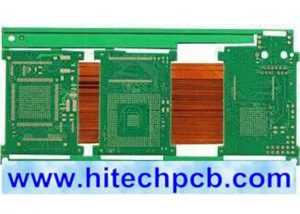
Rigid-flex PCB manufacturer up to 18 layers
What are Rigid-Flex Circuit Boards? <br> <br>As the name implies, a Rigid-Flex PCB is a hybrid of a Flex PCB and a Rigid PCB. The combination of the two types of boards utilises the benefits each one provides, integrating the versatility of the flexible board with the robustness of the rigid board. Rigid-flex printed circuit boards are used in more complex mechanical designs, eliminating flexible cables and wiring and replacing it with integrated circuits. <br> <br>Rigid-Flex PCBs, by definition, are a combination of rigid part(s) joined by interconnecting flex areas where the flex material is used across the entire PCB area. <br> <br>The rigid parts are where there is no bending requirement. Again, PTHs take connections from layer to layer as required. Rigid-flex may also employ other technologies as required eg. HDI. Unlike the cost-effective flex PCBs, Rigid-Flex PCBs can be a bit more costly due to their intricate design. <br> <br>Rigid-flex PCB design can be used to eliminate or greatly reduce requirements for bulky and costly cable harnesses, in turn taking out costs and reducing assembly time. Like the pure flexible PCBs, a high volume of rigid-flex PCBs are used in aviation and space applications – and also in automotive and test equipment. <br> <br>The flexible layers of a Rigid-Flex PCB are buried within the board and penetrate through the rigid sections of the PCB. <br> <br>The trend to miniaturization in electronics continues. Integrated circuit board solutions are becoming more and more popular as a means of efficiently utilizing the even smaller casing volume in all three dimensions. <br> <br>A rigid-flex printed circuit board is unique as the rigid part of the circuitry can be placed directly into the application. Then, the flexible section can be bent and even folded to fit around components to make another direct connection. This aspect ensures a reliable connection to parts for higher performance. <br> <br>Some of the most common products that incorporate rigid-flex PCBs in their design include laptop computers, smartphones, and wearable devices due to the bending capabilities of rigid-flex. <br> <br>Rigid-flex pcb boards are PCBs that have Flexible PCBs (FPC) and Rigid PCBs on the same board, which are commonly employed to save space, remove wiring assemblies and can also be welded with complex components. Combining other higher technology boards, such as HDI, as a part of its packaging, is also a common design. <br> <br>Rigid Flex PCB design <br> <br>The designs of Rigid Flex PCBs are a little more complex as these boards are designed in 3D, which allows the board to be folded or twisted to create the desired shape for the product. Designing a board in 3D means they can offer greater spatial efficiency and can subsequently be used in special instances where space and weight reduction may be necessary, such as in medical devices. By being able to design in three dimensions designers can twist, fold and roll the flexible board substrates to achieve their desired shape for the final application's package. <br> <br>Rigid Flex PCBs are usually thinner than other boards, meaning it’s a great option for any thin or light packaging needs your products may have. With thin copper layers and adhesive-less laminates, it’s a great small, thin and light solution for your circuit design needs. <br> <br>Rigid-Flex PCBs Fabrication Applications: <br> <br>Rigid-Flex PCBs offer a wide array of applications, ranging from smart devices to cell phones and digital cameras. Increasingly, rigid-flex board fabrication has been used in medical devices such as pacemakers for their space and weight reduction capabilities. The same advantages for rigid-flex PCB usage can be applied to smart control systems. <br> <br>In consumer products, rigid-flex doesn't just maximize space and weight but greatly improves reliability, eliminating many needs for solder joints and delicate, fragile wiring that are prone to connection issues. These are just some examples, but Rigid-Flex PCBs can be used to benefit nearly all advanced electrical applications including testing equipment, tools and automobiles. <br> <br>Rigid-Flex PCB and Its Production Process <br> <br>The development of FPC and PCB has spawned a new product that is called rigid-flex PCB. Therefore, rigid- flex PCB is according to the relevant process requirements and through the lamination process to combine rigid board and flex board to form a circuit board with FPC characteristics and PCB characteristics. <br> <br>Because rigid-flex PCB has a variety of complex structural forms, the manufacturing process is also different. Below picture shows the regular rigid-flex PCB and an example for regular stack up design. <br> <br>Rigid flex PCB production is based on below steps: the first step is to process the rigid outer cover layer. The electroplating graphic that needs to be pressed in the outer layer, and then through the CNC milling machine, punching or laser method, routing out or routing the half of depth of the flexible part which is located in rigid layer. Flex board and the rigid outer cover are boned by adhesive sheet. The adhesive sheet has been pre-opened in the flexible part. <br> <br>During the lamination process, if the rigid outer layer uses routing structure, a suitable pressure filling board should be prepared for the flex part. Using a vacuum pressing machine to obtain better press quality, and meanwhile with some auxiliary coating materials, such as PE, etc., so that the pressing process can provide a uniform pressure on the entire board, and make the low -flowing sticky sheet is fully flowing and filling the gap, especially for complex structures. Before adhesion or lamination, appropriate baking should be done as needed to remove moisture. <br> <br>After lamination, the rigid- flex PCB can use a through hole treatment process which is similar to a multi-layer rigid board, the different part is remove drilling dirt. The method of removing drilling dirt depends on what materials used. Like the rigid board, drilling the hole after fully baking, and then use the plasma etching process to remove the residue in the hole wall. Before the plasma is treated, bake is also needed to remove water vapor. Caval polyesterness is generally recommended to not exceed 13um. The pore -plating process of conventional rigid board can be used, but the specific process parameters of the electroplating should be determined according to the reliability test data of the pores. <br> <br>The next process is similar to the multi -layer rigid board. The outer layer etching, covering membrane (welded film), surface treatment, etc. can be used in similar processes. When making outline of the rigid-flex PCB, remove the filling board in the flexible part or depth control rigid outer cover in the flexible area can be formed into a rigid-flex PCB. <br> <br>Careful consideration of Rigid-Flex solutions and a proper assessment of the available options at the early stages in the rigid-flex PCB design phase will return significant benefits. The Rigid-Flex PCBs fabricator must be involved early in the design process to ensure the design and fab portions are both in coordination and to account for final product variations. <br> <br>The Rigid-Flex manufacturing phase is also more complex and time-consuming than rigid board fabrication. All the flexible components of the Rigid-Flex assembly have completely different handling, etching, and soldering processes than rigid FR4 boards. <br> <br>Benefits of Rigid Flex PCB <br> <br>Space requirements can be minimized by applying 3D <br> <br>By removing the need for connectors and cables between the individual rigid parts the board size and overall system weight can be reduced. <br> <br>By maximizing space, there is often a lower count in parts. <br> <br>Less solder joints assure higher connection reliability. <br> <br>Handling during assembly is easier in comparison with flexible boards. <br> <br>Simplified PCB assembly processes. <br> <br>Integrated ZIF contacts provide simple modular interfaces to the system environment. <br> <br>Test conditions are simplified. A complete test prior to installation becomes possible. <br> <br>Logistical and assembly costs are significantly reduced with flex-rigid boards. <br> <br>It is possible to increase the complexity of mechanical designs, which also improves the degree of freedom for optimized housing solutions. <br> <br>Rigid Flex PCB Fabrication Applications <br> <br>Rigid flexible PCBs offer a wide array of applications, ranging from military weaponry and aerospace systems to cell phones and digital cameras. Increasingly, rigid flex board fabrication has been used in medical devices such as pacemakers for their space and weight reduction capabilities. The same advantages for rigid flex PCB usage can be applied to military weaponry and weapon control systems <br> <br>In consumer products, rigid flex doesn't just maximize space and weight but greatly improves reliability, eliminating many needs for solder joints and delicate, fragile wiring that are prone to connection issues. These are just some examples, but rigid flex PCBs can be used to benefit nearly all advanced electrical applications including testing equipment, tools and automobiles. <br> <br>Available structures for rigid flex PCB <br> <br>There are numerous, different structures available. The more common ones are defined below: <br> <br>Traditional rigid flex construction (IPC-6013 type 4) Multilayer rigid and flexible circuit combination containing three or more layers with plated through holes. <br> <br>Asymmetrical rigid flex construction, where the FPC is situated on the outer layer of the rigid construction. Containing three or more layers with plated through holes. <br> <br>Multilayer rigid flex construction with buried / blind via (microvia) as part of the rigid construction. 2 layers of microvia are achievable. Construction may also include two rigid structures as part of a homogeneous build. <br> <br>Rigid Flex Printed Circuit Board Manufacturer <br> <br>Rigid flex printed circuit boards (PCBs) are manufactured by combining rigid and flexible board technologies. These circuit boards are made up of multiple flexible circuit inner layers. An epoxy pre-preg bonding film is used to attach together these inner layers. The key benefit of these boards is that they are a combination of the best quality of flexible and rigid circuit boards. This can have several further benefits as far as stability, assembly, signal transmission, and overall size of the circuit are concerned. Hitechpcb provides a number of variants in rigid flex PCBs, which include 4 layer rigid flex with ENIG finish, 10 layer rigid flex with 4 layer flex, 12 layer rigid flex with heat sink, 14 layer rigid flex circuit boards, and many more. It is one of the leading rigid flex PCB manufacturers. <br> <br>Every printed circuit board depends on the copper for carrying electricity. We understand that copper thickness plays a key role in the performance of these circuit boards. Thus, we allow the customers to choose from a variety of copper thicknesses, including 0.5 OZ, 1.0 OZ, 2.0 OZ, 3.0 OZ, up to 6 OZ. The solder mask helps in improving the aesthetic appeal of the components on the PCB. We can provide rigid flex printed circuit boards in various solder mask colors, including white, black, blue, green, red, and Taiyo PSR4000 white. The PCB can be availed in silkscreen colors – black and white. <br> <br>Rigid flex printed circuit boards have minimal space requirements that are optimized by 3D application. These circuit boards require no cables or connectors between the rigid parts. This helps reduce the board size, as well as overall system weight. These lesser solder joints also help assure high connectivity. Additionally, these boards have ZIF contacts that are integrated. These contacts help simplify the system interfacing. This 4 layer rigid flex PCB and other printed circuit boards are vacuum packed during the transit. This helps us assure the quality, as well as working condition of the boards. <br> <br>The Disadvantage and Advantage of Rigid-Flex PCB <br> <br>Rigid-flex PCB has many production processes with the characteristic of superior difficulty in production and high defect rate. Its biggest disadvantage is that the price is more expensive than flex PCB or rigid PCB and long production cycle. Another disadvantage is that both SMT and furnaces may need to use carrier to support the flex PCB which virtually increases the SMT cost. <br> <br>One of the key features of rigid-flex PCB is the thin profile and changeable shape, making it an ideal solution for ultra -thin and ultra -light packaging. Although the rigid flex PCB may be more expensive in design and manufacturing, they do have many advantages and can solve many problems in traditional hardboard technology. <br> <br>1. Small Size and Flexible Shape <br> <br>The rigid- flex PCB is easier to install more components in smaller space, because they can change the shape according to a specific contour. This technology will reduce the size and weight of the final product and the overall system cost. At the same time, the compact shape of rigid flex PCB makes it the best choice for fine lines and high -density circuits in HDI technology. <br> <br>2. Customized for Different Applications <br> <br>Rigid-flex PCB has various packages, which can be customized for the application of many industries such as aerospace, military, medical equipment and consumer electronics. They can customize the size and shape to adapt to the shell design and 3D design, which provides designers with more possibilities to meet different requirements in specific applications. <br> <br>3. Better Mechanical Stability <br> <br>The stability of the rigid board and the flexibility of the flexible board form the stable structure of the entire packaging, while retaining the reliability and flexibility required for small space installation. <br> <br>4. Good Performance in Harsh Environments <br> <br>Rigid-flex PCB has high resistance and high vibration capacity, so they can work normally in a high -stress environment. There are fewer cables and connectors used in rigid-flexible PCB, which also reduces security risks and maintenance in future use. <br> <br>5. Easy to Manufacture and Test <br> <br>The rigid-flex PCB requires a small number of inter connect and related components/parts. It helps simplify the assembly operation, making rigid –flex PCB easier to assemble and test. Rigid-flex PCB is very suitable for PCB prototypes. <br> <br>In addition to the above advantages, other common advantages of rigid-flex PCB also include high circuit density, good heat dissipation and good chemical resistance. In a word, rigid-flex PCB combines all the advantages of rigid PCB and flex PCB, and at the same time make up for the shortcomings. This PCB is the best solution to design reliable and powerful circuits for smart wearable devices and other industries. <br> <br>[a]https%3A%2F%2Fwww.hitechpcba.com%2Frigid-flex-pcb-manufacturer[/a]
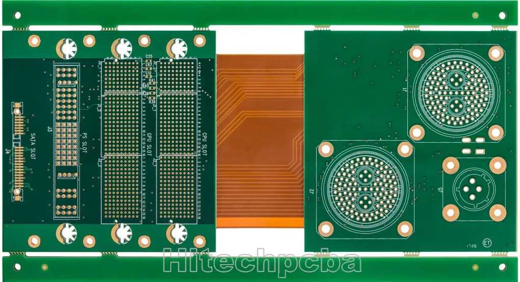
Rigid flex pcb board
What is rigid flex pcb board? <br> <br>Rigid-flex PCB board, it is a circuit board that combines flexible and rigid circuit board technology in the application. Most rigid-flex boards are composed of multiple layers of flexible circuit boards, which are attached to one or more rigid boards from the outside and/or from the inside, depending on the design of the application. The flexible substrate is designed to be in a constant deflection state, and is usually formed as a deflection curve during rigid flex pcb manufacturing or assembly. <br> <br>Hitech rigid flex pcb manufacturing process <br> <br>After the production of FPC flexible boards is completed, the production of Hitech rigid flex pcb boards can be completed through the following processes. <br> <br>1. Punching <br> <br>Drill holes on FR4 and PP film, and the design on the alignment hole is not the same as the general through hole. After the punching is completed, browning is required. <br> <br>2. Riveting <br> <br>Laminate copper clad laminates, PP adhesives, and FPC circuit boards and place them neatly. The original old process is to laminate and pressing step by step, but it is a waste of time. After many attempts, we found that the stacking process can be completed once. <br> <br>3. Laminate <br> <br>This is a relatively complete step in the production of rigid-flex pcb board. Most of the materials are integrated for the first time. First, the bottom layer is copper clad laminate and PP film, above are the FPC flexible board produced in the previous process, and a PP film is placed on the FPC flexible board, then place the last layer of copper clad laminate. All materials to be laminated are placed in order and pressed together. <br> <br>4. Trimming <br> <br>That is to remove the part of the circuit board where there is no circuit at the edge of the circuit board currently and in the future. Afterwards, it is necessary to measure whether the material has excessive expansion and contraction. Because the PI used in the production of flexible boards is also expansion and contraction, this has a very large impact on the production of circuit boards. <br> <br>5. Drilling <br> <br>This step is the first step to turn on the entire circuit board, and the production parameters should be produced according to the design parameters. <br> <br>6. Desmear <br> <br>First, remove the scum generated by the drilling of the circuit board, and then use plasma cleaning to clean the through holes and the board surface. <br> <br>7. Immersion copper <br> <br>This step is the process of electroplating through holes, also known as hole metallization. Realize through-hole power conduction. <br> <br>8. Plate plating <br> <br>Partially electroplating copper on the upper surface of the electroplating hole makes the copper thickness above the through hole exceed a certain height of the copper clad board surface. <br> <br>9. Outer dry film positive film production <br> <br>The same as the production process of the anti-corrosion dry film of the FPC board, the circuit to be etched on the copper clad board is made. After the development is completed, check the circuit. <br> <br>10. Graphic plating <br> <br>After the initial copper sinking, pattern electroplating is performed, and the current time and copper plating wire are used according to the design requirements to reach a certain electroplating area. <br> <br>11. Alkaline etching <br> <br>12. Print solder mask <br> <br>This step has the same effect as the FPC board protective film. We see that the PCB rigid board is generally green. This step is generally called green oil printing. After the printing is completed, the inspection is carried out. <br> <br>13. Open the cover <br> <br>Cover opening, which is the area where the FPC board is located, but the area not needed by the rigid board is laser cut to expose the FPC board. <br> <br>14. Curing <br> <br>It is also a baking process. <br> <br>15. Surface treatment <br> <br>Generally, at this time, a rigid-flex PCB board has been manufactured, and only the metallization treatment is required on the surface of the circuit board, which can play a role in preventing wear and oxidation. Generally, this process is to soak the circuit board in a chemical solution, and the metal elements in the solution are densely distributed on the circuit board circuit. <br> <br>16. Characters printing <br> <br>The positions of the parts to be assembled and some basic product information are printed on the rigid-flex board in the form of characters. <br> <br>17. Test <br> <br>This is a process of checking whether the circuit board is qualified. The test items are tested for electrical properties according to customer requirements. The tests generally include impedance test, open and short circuit test and so on. <br> <br>18. Final inspection <br> <br>19. Packaging and shipping <br> <br>There are many ways to package circuit boards. Generally, Hitech use packaging bags to separate them, and then use a vacuum packaging machine to vacuum package the rigid-flex PCB boards . <br> <br>The advantages of rigid-flex PCB board <br> <br>1). It can effectively save the space on the circuit board and eliminate the use of connectors <br> <br>Because the FPCB and rigid pcb board has been combined, the space that originally needed to use the connector can be saved. For some circuit boards with high-density requirements, less connectors will be better. In this way, it also saves the cost of parts using the connectors. In addition, the space between the two boards can be made tighter by eliminating the need for connectors. <br> <br>2). The signal transmission distance is shortened and the speed is increased, which can effectively improve the reliability <br> <br>The traditional signal transmission through the connector is “circuit board→connector→flexible pcb board→connector→circuit board”, while the signal transmission of the rigid-flex PCB board is reduced to “rigid circuit board→flexible pcb board→rigid circuit board”, signal transmission distance between different media is shortened, and the problem of signal transmission attenuation between different media is also reduced. Generally, the circuit on the PCB board is made of copper, while the contact terminal of the connector is gold-plated, and the solder pin is fully tin-plated. Moreover, solder paste is required to be soldered on the circuit board, and the signal transmission between different media will inevitably be attenuated. If you switch to a rigid-flex PCB board, these media will become less, and the signal transmission ability can be relatively improved. For some products that require higher signal accuracy, it helps to improve their reliability. <br> <br>3). Simplify product assembly and save assembly time <br> <br>The use of a rigid-flex PCB board can reduce the man-hours for SMT parts, because the number of connectors is reduced. It also reduces the man-hours for assembly of the whole equipment, because it eliminates the assembly action of inserting the FPC board into the connector. It also reduces the cost of parts management and inventory, because the required parts is reduced, so the management cost becomes less. <br> <br>The disadvantages of rigid-flex PCB boards <br> <br>The biggest disadvantage of the rigid-flex PCB board is that the price of “rigid-flex PCB board” is more expensive, and it may be nearly double the original price of pure “FPC board + rigid PCB board”, but if the price of the connector and processing cost is deducted, the price may tend to be the same, and the detailed cost may have to be actuated to have a clearer outline. <br> <br>Another disadvantage is that it may need to use a carrier to support the part of the FPC board for both the production and the furnace, which invisibly increases the assembly cost of the SMT. <br> <br>Applications of rigid-flex PCB boards <br> <br>The rigid-flex PCB boards provide a wide range of applications from smart devices to mobile phones and digital cameras. Rigid-flex board manufacturing has been increasingly used in medical devices such as pacemakers to reduce their space and weight. The use of rigid flexible PCB has the same advantages and can be applied to intelligent control systems. <br> <br>FAQs on Rigid-Flex PCBs at Hi-Tech Circuits <br> <br>1. Can Hitech Circuits customize Rigid-Flex PCBs for specific applications? <br>Absolutely! Hitech Circuits specializes in customizing Rigid-Flex PCBs to meet specific design requirements and applications. Our team works closely with clients to ensure the final product meets their exact specifications. <br> <br>2. Are there any limitations to the design of Rigid-Flex PCBs? <br>While Rigid-Flex PCBs offer great flexibility and versatility, there are some limitations in terms of maximum size and complexity due to manufacturing constraints. However, our team is experienced in overcoming these challenges to meet client needs. <br> <br>3. What is the typical lead time for a Rigid-Flex PCB project? <br>Lead times can vary depending on the complexity of the design and the specific requirements of the project. Generally, it ranges from a few weeks to several months. We prioritize efficient production while maintaining high-quality standards. <br> <br>4. How does Hitech Circuits ensure the quality of their Rigid-Flex PCBs? <br>Quality assurance is integral to our process. We conduct rigorous testing and inspection at every stage of production, from raw materials to the final product, ensuring that each PCB meets our high standards and client expectations. <br> <br>[a]https%3A%2F%2Fhitechcircuits.com%2Fpcb-products%2Frigid-flex-pcb%2F[/a]

Tìm hiểu về Euro 2024
Tháng 6 năm nay giải đấu vô địch bóng đá các quốc gia châu u (Euro) sẽ được khởi tranh, hôm nay anh em hãy cùng Vegas79 tìm hiểu về giải đấu năm nay. <br>XEM THÊM >> EURO 2024 VEGAS79 <br>[a]https%3A%2F%2Fvegas79.sale%2Feuro-2024-khi-nao-dien-ra-tat-tan-tat-ve-euro-2024%2F[/a] <br>Giải vô địch bóng đá châu u 2024 (hay UEFA Euro 2024), thường được gọi là Euro 2024, là Giải vô địch bóng đá châu u lần thứ 17, giải vô địch bóng đá quốc tế nam 4 năm một lần của các đội tuyển quốc gia châu u được tổ chức bởi Liên đoàn Bóng đá Châu u (UEFA). <br>Vòng chung kết sẽ diễn ra tại 10 quốc gia trên khắp châu u từ ngày 14 tháng 6 đến ngày 14 tháng 7 năm 2024. Trận chung kết sẽ được diễn ra tại Sân vận động Olympic ở Berlin, Đức. <br>Vòng loại đã diễn ra từ tháng 3 năm 2023 đến tháng 3 năm 2024, với 53 đội tuyển quốc gia châu u tranh 24 suất tham dự vòng chung kết. <br>Đương kim vô địch là đội tuyển Ý, họ đã giành chiến thắng trong trận chung kết Euro 2020 trước đội tuyển Anh. <br>Dưới đây là một số thông tin thú vị về Euro 2024: <br>Đây là lần đầu tiên Đức đăng cai một kỳ Euro kể từ năm 1988. <br>Đây là lần đầu tiên một kỳ Euro được tổ chức tại 10 quốc gia. <br>Đây là kỳ Euro đầu tiên có 24 đội tham dự. <br>Sẽ có một số sân vận động mới được xây dựng hoặc cải tạo cho giải đấu, bao gồm Sân vận động Olympic ở Berlin và Sân vận động Allianz ở Munich. <br>Mascot của giải đấu là Scatori, một chú sóc đỏ đại diện cho sự nhanh nhẹn, thông minh và tinh thần thể thao. <br>Chắc chắn rồi, đây là một số thông tin bổ sung về Euro 2024: <br>Dưới đây là một số thông tin thú vị bổ sung về Euro 2024: <br>Giải đấu sẽ sử dụng loại bóng mới, Adidas Conext21 , được thiết kế để có độ chính xác cao hơn và có đường bay ổn định hơn. <br>Giải đấu sẽ có hệ thống VAR mới, được sử dụng để xem xét các quyết định trên sân. <br>Giải đấu sẽ là giải đấu đầu tiên sử dụng hệ thống việt vị bán tự động , sử dụng camera và trí tuệ nhân tạo để giúp trọng tài đưa ra quyết định việt vị. <br>Giải đấu sẽ là giải đấu đầu tiên sử dụng hệ thống việt vị kết hợp , hệ thống này sẽ kết hợp hệ thống việt vị bán tự động với trọng tài việt vị truyền thống. <br>Tôi hi vọng thông tin này hữu ích. Vui lòng cho tôi biết nếu bạn có bất kỳ câu hỏi nào khác.
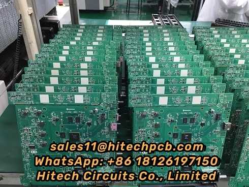
Your leading PCB High Volume PCB Assembly supplier in China
Your leading PCB High Volume PCB Assembly supplier in China <br> <br>With 15 years of experience and high efficiency in PCB assembly and manufacturing, HITECH CIRCUITS is the perfect source for Big Batch PCB assembly on a limited budget. If you are looking for a large PCBA assembly within your budget, we will be your ideal choice. HITECH CIRCUITS has more than 15 years of experience in the OEM/PCBA manufacturing and assembly of printed circuit boards, advanced production technology and equipment, professional engineers and purchasing team to provide our partners with personalized and complete process solutions. HITECH CIRCUITS’s supply chain services deliver supply chain innovation on demand. We offer a bold, yet proven service solution designed to grow market share and profit. Our innovative approach to managing the supply chain offers a complete business model that delivers the talent and transformative tools necessary to create predictability, reliability, and responsiveness across your entire supply chain. Our practitioners are passionate about supply chains. We have spent a generation understanding, refining and building the best in intelligent supply chains. We provide talent on-demand with expertise in data analytics and strategic technologies that can help you predict, plan and respond more effectively. <br> <br>Some designs require assemblies in small volume, maybe just prototypes, while others require them in high volume. At SMT house, High Volume, Large Volume, or Big Batch PCB Assembly always refers to printed board assembly projects with quantities more than 5K pieces. HitechPCB has the capability to offer high volume PCB assembly services to meet your requirements of high-quality, competitive price, on-time delivery and smooth communication in any manner of full turnkey, consigned and partial turnkey. <br> <br>Also, if your business is involved in applications that require high-volume PCB assembly, the company to contact is HitechPCB, because we’re a complete turnkey solution for printed circuit boards assembly, we are ideally suited for bulk PCB assembly orders. Our state-of-the-art equipments, large facility and wide range of highly-qualified experts give us the capability of high-volume PCB assembly of up to 9,000,000. <br> <br>We are also the perfect source if you’re looking for large-order PCB assembly on a budget. Because of our high level of efficiency and more than 10 years of experience with printed circuit board manufacturing and electronics assembly, we offer large printed circuit board orders at surprisingly competitive prices compared to other PCB manufacturers or PCB assembly companies. <br> <br>Our large order PCB assembly process starts with a tested and practiced set of workflow guidelines for every phase of the process, from pre-order PCB design consultation with professional veteran engineers to PCB fabrication, components sourcing, PCB assembly, PCBA testing, PCBA inspection, PCBA packing and shipping all under the auspices of a highly-skilled production staff. You can be confident that no matter how many circuit boards you order, you will enjoy fast service, low prices and extremely high quality. <br> <br>With our excellent after-sales service, 24 sales and technical support team, quick response service, we will be your best Big Batch PCB assembly manufacturer inChina. A wide variety of highly qualified experts <br> <br>Why choose Hitechpcba Big Batch PCB Assembly <br>Compared to our competitors, Hitechpcba offers large printed circuit board orders at very competitive prices. The risky big batch PCB assembly process begins with a set of tried and tested workflow guidelines. From ordering PCB design to component procurement, manufacturing, testing, assembly, inspection, shipping and packaging. This is all under the guidance of our highly skilled production staff. <br> <br>No matter how many boards you order, you'll love the fast response service, low cost, and surprisingly high quality. <br> <br>Whether you are seeking for product designer, electrical engineer, system integrator, manufacturer, or big batch PCB manufacturing and assembly, low cost big batch PCB housing, electronic assembly services, Hitech Circuits PCB Assembly team will be your perfect choice for big batch PCB assembly plant inChina. <br> <br>Finding Reliable High Volume PCB Assembly Supplier? <br> <br>When your design passed the prototyping verification after optimization, DFM and DFT check, it’s time to find a manufacturer or a supplier who has ability to perform high volume PCB manufacturing and assembly for you. HITECH CIRCUITS is a one-stop PCB solution provider, no matter which your design stage is located, we always can help in PCB manufacturing, assembly and design. With both design and manufacturing knowledge, we can feedback some suggestions to modify or change your design on the basis of cost-down without sacrificing the quality and performance. What’s more, if choosing our full turnkey PCB assembly service, we will be responsible of BOM sourcing to reduce your workload. Our approach to conducting high volume printed circuit board assembly is founded on a commitment to the highest possible quality, based on IPC standards and our inner quality control processes. In spirit of those high assembly standards, HITECH CIRCUITS developed excellent high-volume assembly capabilities and manufacturing processes relied on our advanced assembly lines in dust-free workshop. <br> <br> <br>What is big batch PCB assembly? <br> <br>Big batch PCB assembly is an assembly process where you will assemble 10,000 or more PCBs in a specific period of time. The main processes you will use to assemble PCBs in large quantities are design for manufacturing and design for testing. <br> <br>What are the advantages of using big batch PCB assembly? PCB assembly process <br> <br>With applications in mind, big batch PCB assembly will provide you with numerous industrial and personal benefits. This is why electronic OEM prefer to use it in most of their applications. <br> <br>The following are the main advantages of using mass printed circuit components: <br> <br>Rapid design and prototyping process <br>Since you will be mass-producing or manufacturing printed circuit boards, you must assemble them uniformly. By simply creating a design and a prototype that works for each PCB, you can save a lot of time. <br> <br>Short production cycle <br>Since the production process is fully automatic, you will also save time in the production of numerous PCBS. It all starts with the design and prototyping phase, which you'll do with the help of software and machines. <br> <br>Production consistency <br>You will also have a very uniform production process because most of the details are predetermined before implementation. Once production begins, all manufacturing specifications will follow uniform specifications for all printed circuit boards. <br> <br>Quality consistency <br>Since you will be producing all PCBs to similar specifications, you will automatically get consistent quality throughout the production process. In other words, you should rest easy knowing that you will have consistency across all printed boards. <br> <br>First-class cost performance <br>This is the most convenient model for the cost of producing printed circuit boards because you can do everything very consistently. Here, you will buy all the materials in bulk and produce them in a short time using similar machines. <br> <br>Improve the market's ability to time <br>You will be able to produce large number of printed circuit boards in a very short time, thus giving you the advantage in the market. In other words, you will have a steady supply of on-demand printed circuit boards, giving you the advantage in the market. <br> <br>Do you have lead-free mass PCB assembly? <br>Yes, we care about the health of our users and the health of the environment. We are aware of the harmful or negative effects that lead emissions can have on users and the environment.That's why we eliminate lead from production materials. It is of great benefit to protect people's health and eliminate environmental pollution. <br> <br>What is the testing protocol for mass PCB assembly? <br>As long as you have completed the process of producing printed circuit boards, you must ensure that they run well. <br> <br>Existing testing protocols will help ensure that large volumes of PCBs are in perfect working condition. <br> <br>Here are the main test protocols you can perform on a high volume printed circuit board: <br> <br>Automated Optical Inspection (AOI) <br>You will use Automated Optical Inspection (AOI) tools to accurately and efficiently detect production errors in big batch PCB assembly. It has cameras and image-processing software that can identify assembly errors and relay information for further action. It is the best tool you will use for better error detection than visual inspection. <br> <br>Solder Paste Inspection (SPI) <br>After you have finished printing with the paste printer, you must pass it through the paste inspector. The SPI machine has a camera and communication system equipment that can examine every detail of the solder paste.It compares these details to the Gerber file and reports any kind of inconsistency. <br> <br>In-Circuit Test (ICT) <br>In-Circuit Test, you can use the most detailed test methods to check the quality and integrity of the PCB.Here, you will have to take personal initiative and use online testing software to check the quality of your PCB.You will use the machine to detect errors in the PCB for correction. <br> <br>Functional Circuit Test <br>Here, you will use a computer with test pins or test probes to test the functional integrity of the PCB. You can tell if the board passes the test simply by comparing the results to the design specifications. <br> <br>X-ray Examination <br>You will use X-ray inspection to detect welding problems on the PCB that are not visible to the human eye. Here, you do not have to cut through the circuit board to see the welding quality on the printed circuit board. You'll use X-ray inspection protocols to detect errors in components and soldering on circuit boards. <br> <br>Do you have a custom mass PCB assembly? <br>Yes, we do customize mass printed circuit boards. <br>You can order the most unique types of printed circuit boards and we will produce them according to your needs. <br>We'll review your design, create a prototype, and then test how it works. <br>Once we confirm that it is working well according to the design details, we will proceed with the production process. <br> <br>How does small batch PCB assembly compare to large batch PCB assembly? <br>On the production scale, you can choose between large batch PCB assembly or small batch PCB assembly. <br>Mass PCB assembly is the process by which you assemble 10,000 or more printed circuit boards. <br>It is a mass production or assembly system that can mass produce PCBs in a short period of time. <br>On the other hand, you can choose to assemble PCBs in small batches for small scale production or assembly of PCBs. <br>In other words, you will produce a very small number of printed circuit boards of 250 or less. <br>In large and small batch PCB assembly, the assembly process will remain the same. <br>In addition, you will use similar detection techniques for high - and small-lot PCB assemblies. <br> <br>What are the main capabilities of mass PCB assembly? <br>Well, when you're looking for a good large volume PCB assembler, there are some special features. <br>This means that they must have the specific resources that you will use in the PCB assembly process. <br>The following are the main functions that must be available for mass PCB assembly. <br> <br>Manufacturing capacity <br>It is important to have a manufacturer that can use both surface mount technology and through-hole technology. <br> <br>You must find a manufacturer with sufficient knowledge and experience in surface mount technology and through-hole technology. <br> <br>Fast turnaround time <br>You should also have a manufacturer that can produce large number of PCBs in a very short time. <br>In other words, you don't have to wait longer to get the printed circuit board you ordered. <br> <br>Welding capacity <br>In this case, the key point you must pay close attention to is the ability to weld manually and by machine. Your manufacturer should be able to perform both hand and machine welds. <br> <br>Quality compliance <br>You should also know that the quality of the printed circuit board is a top priority when it comes to durability and safety. <br>Here, your manufacturer must have the knowledge to read the list of materials and identify the right quality products. <br> <br>Test method <br>You must also choose a manufacturer that has knowledge of all test machines and printed circuit boards. <br>In other words, after production, your supplier must test all printed boards accordingly before providing PCBs. <br> <br>What are the applications of mass PCB assembly? <br>You will be mass-producing large volume PCB assemblies of different equipment at high rates. <br>If you want to enter the PCB production market, you must have knowledge of mass PCB assembly. <br> <br>Here are some industries that require big batch PCB assembly. <br>The communications industry mass-produces communications equipment <br>Military or defense industry <br>Automobile industry <br>Aviation industry <br>You will be using big batch PCB assembly in an industry where big batch production, consistency, and consistency are important. <br> <br>What is the cost of mass PCB assembly? <br>Well, the cost of mass-producing printed circuit boards is fairly affordable. <br>Here, you will apply economies of scale in the production process, thereby reducing the cost of producing PCBs. <br>In addition, other factors that affect cost such as quality and size will also play an important role. <br>You will spend more on high quality and larger PCB materials, increasing production costs. <br>Typically, the amount you will spend usually depends on the design specifications of your PCB. <br> <br>How safe is the mass PCB assembly process? <br>Well, most of the manufacturing process for big batch PCBs is highly automated. <br>In other words, there was little human involvement other than the design and programming of the machine. <br>In addition, we eliminate any material that would suspend harm to the environment and users. <br>This makes mass PCB assembly one of the safest modes for producing printed circuit boards. <br> <br>Do you provide both THT and SMT in big batch PCB assembly? <br>Yes, we have both through-hole technology and surface mount technology for PCB assembly. <br>These are the main manufacturing methods we use to produce high quality printed circuit boards. <br>You will choose among these manufacturing modes based on the design and application specifications. <br> <br>Is there turnkey assembly for large volume PCB assembly? <br>Of course, our production system is capable of handling very large volumes of turnkey PCBs. <br>You'll find products that you can buy in bulk to meet your production needs. <br>Here, we will be responsible for every step of production from design, inspection, prototyping and assembly. <br>What is the turnaround time for mass PCB assembly? <br>You should rest easy knowing that your production specifications will be met as planned. <br>This includes time for all production specifications and you will accordingly meet all your market needs. <br> <br>What are the quality certifications for mass PCB assembly? <br>As we mass-produce printed circuit boards, we also ensure consistent quality. <br>This means that you will get the highest quality printed circuit boards in large quantities at an affordable price. <br>Our quality meets and exceeds international quality standards, namely: <br>Comply with IPC quality standards such as IPC-WHMA-A-610 and IPC-CC-830B <br>ANSI/AHRI quality standards, such as ANSI/J-STD-001 -- Class II and III only <br>RoHS quality certification <br>UL quality standard <br>CE quality standard <br> <br>What to consider when choosing big batch PCB assembly services? <br>You'll see the manufacturing capabilities of high-volume PCB assemblers. <br>Here are the main factors that you must pay close attention to: <br>Manufacturing and service capabilities <br>QC <br>Years of manufacturer experience <br>Customization capability <br>Turnaround time <br>Responsiveness and flexibility <br>Delivery service <br> <br>Why is it difficult to scale up from prototype to high-volume assembly? <br>Scaling up from low-volume to high-volume PCB assembly can prove to be a difficult and painful process. <br>Here are the main reasons why this can pose a difficult challenge. <br>You must change design files and formats to meet new design requirements <br>You may also lack the correct type of machine for the new specification <br>You may also have to change components that will be tied to the PCB <br>You may also have to change the entire design to accommodate the new specifications <br>How do you simplify the transition from prototyping to high-volume PCB assembly? <br>Despite the difficulties, you should rest easy knowing that you can easily complete the process. <br>The best way is to choose the best prototype CM that can collaborate all the details accordingly. <br>It will help remove obstacles that can cause confusion and make the process difficult. <br> <br>At Hitech Circuits, we will help you with the PCB fabrication and PCB assembly process. <br>Contact us today for all of your big batch PCB assembly needs. <br> <br>Parts Quality Guarantee and Reliable Testing Methods <br> <br>For verifying your turnkey orders, HITECH CIRCUITS would like to provide Prior PCB assembly service, which we will assemble 3-5pcs of your PCBs ahead of the main assembly production run, and ship these prior PCBAs to you for testing. This service is totally free of charge and only available for full turnkey PCB assembly orders in high volumes, which means HITECH CIRCUITS handling PCB fabrication, Components sourcing, and final assembly for your project. In this way, you can work with our assembly team to ensure that the finished product exactly meets your specifications every time. No one knows your design as well as you do, and so we offer prior Electronics Manufacturing assembly service as a guarantee that each and every board leaving our PCB and SMT facilities will meet your own personal standards in quality and performance. Of course, this is flexible threshold; we also would like to provide prior PCB assembly service for some smaller orders if they incorporate a high degree of complexity. Prior PCB assembly is especially popular among our customers who require IC programming services, since it allows for them to ensure that their source code will function as expected on the finished assembled boards, before their full order is assembled. <br> <br>For further details freely contact Cynthia at [email protected] <br>[a]https%3A%2F%2Fwww.hitechpcba.com%2Fhigh-volume-pcb-assembly[/a]
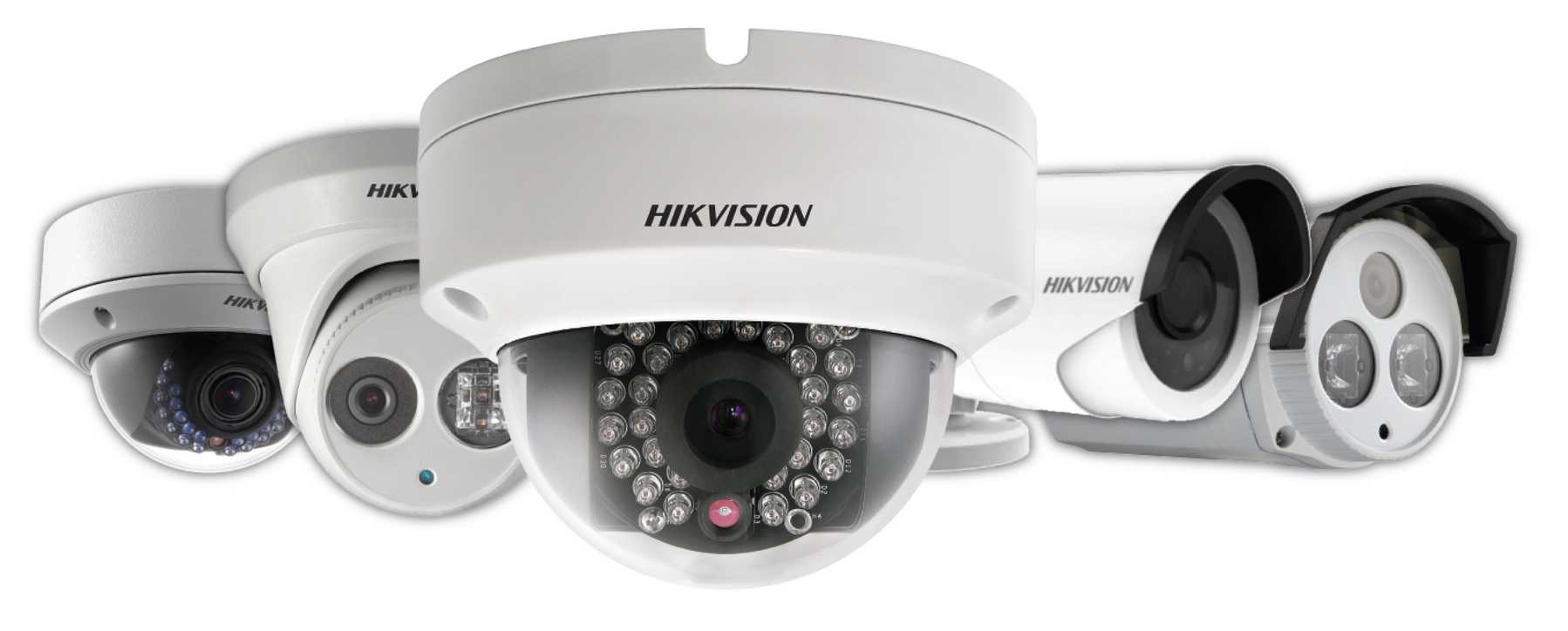
Ayush Infotech
Elevate your security with Ayush Infotech, the premier HikVision CCTV camera dealer in Jaipur. Explore advanced surveillance solutions for residential, commercial, and industrial properties today.
Tools and Equipment
In the automotive industry, numerous tools and equipment are used for various purposes, including repair, maintenance, and manufacturing. Here are some of the commonly used tools and equipment: <br>1. Hand tools: <br> - Wrenches (open-end, box-end, combination, ratcheting), Sockets and ratchets, Screwdrivers (flat-head, Phillips, Torx, etc.), Pliers (slip-joint, locking, needle-nose, etc.), Hammers (ball-peen, dead-blow, rubber mallet), Pry bars and trim removal tools, Wire strippers and crimpers <br>2. Power tools: <br> - Impact wrenches (air or electric), Drills (corded or cordless), Grinders (angle grinders, die grinders), Saws (reciprocating, circular, jigsaw), Pneumatic tools (air ratchets, air hammers, air chisels) <br>3. Diagnostic tools: <br> - Scan tools (OBD-II scanners, code readers), Multimeters, Circuit testers, Compression testers, Vacuum gauges, Timing lights, Borescopes and inspection cameras <br>4. Lifting and jacking equipment: <br> - Floor jacks, Jack stands, Hydraulic lifts (two-post, four-post, in-ground), Engine hoists and cherry pickers <br>5. Specialty tools: <br> - Pullers (bearing, gear, etc.), Brake tools (caliper compressors, brake bleeders), Torque wrenches, Locking pliers (Vise-Grips), Wheel alignment equipment, Tire changers and balancers <br>6. Lubrication and fluid transfer equipment: <br> - Grease guns, Oil drain pans, Fluid transfer pumps, Funnels and pour spouts <br>7. Shop equipment: <br> - Workbenches and tool chests, Parts washers, Air compressors, Welding equipment, Hydraulic presses <br>These tools and equipment are essential for professionals working in automotive repair shops, dealerships, and manufacturing facilities to perform their tasks efficiently and safely.
SOLAR LIGHT FOR FARM
[a]https%3A%2F%2Fwww.css-solar.com%2Fsolar-light-for-farm.html[/a] <br> <br>Outdoor solar powered farm lights are mainly used in farms, industrial parks, main traffic intersections, and other areas. <br> <br>Normally, solar lights for farmhouse will be equipped with a monitoring function, which can monitor the situation in a certain range in real-time according to the needs of customers. <br> <br>And now solar-powered farm lights are basically high-definition monitoring cameras, with WiFi + 4G function. Under any condition, a solar light for farm is recorded within the range. In some large farms, manors, and industrial parks, you can often spot solar powered lights wholesale for farmhouses. <br> <br>Outdoor solar farm lights not only provide lighting needs but also meet the monitoring and recording needs of most customers. The solar power system is also available, which saves a lot of expenses for many farmers, such as cable laying and pipe laying. <br> <br>Solar Light For Farm Advantages <br>Outdoor solar farm lights, also known as solar-powered farm lights, offer several advantages over traditional lighting systems. Here are some of the key benefits of using solar-powered lights on farms: <br> <br>Cost savings: One of the most significant advantages of using outdoor solar farm lights is the cost savings. Since they are powered by the sun, they don't require electricity from the grid, which can be expensive. This means that you can significantly reduce your electricity bills and save money in the long run.
Security installation in canberra and brisbane
Newhams: Security installers in Brisbane are professionals who specialize in the installation, maintenance, and servicing of security systems for residential, commercial, and industrial properties in the Brisbane area. These systems can include CCTV cameras, alarm systems, access control systems, intercoms, and monitoring services. <br> <br>Security installers in Brisbane typically offer a range of services tailored to the specific needs of their clients. This can include: <br> <br>Consultation and Assessment: They assess the security needs of a property and provide recommendations on the most suitable security solutions based on factors such as location, property layout, and budget. <br> <br>Installation: They install security systems efficiently and effectively, ensuring that all components are properly configured and integrated for optimal performance. <br> <br>Maintenance and Servicing: They offer regular maintenance services to ensure that security systems are functioning correctly and are up to date with the latest technology and security standards. This can include system checks, software updates, and hardware replacements as needed. <br> <br>24/7 Monitoring: Many security installers in Brisbane offer 24/7 monitoring services, where security professionals monitor the property remotely for any signs of unauthorized activity or security breaches. In the event of an alarm trigger, they can quickly respond and dispatch appropriate authorities if necessary. <br> <br>Customer Support: They provide ongoing customer support to address any questions or concerns that clients may have regarding their security systems. This can include troubleshooting, training on system usage, and assistance with system upgrades or expansions. <br> <br>Overall, security installers in Brisbane play a crucial role in helping individuals and businesses protect their properties and assets against various security threats, providing peace of mind and ensuring a safe and secure environment.
Best Makeup Artist in Jaipur
Looking for the epitome of beauty transformations in Jaipur? Look no further than the best makeup artist in Jaipur! With a skillful touch and an eye for detail, they weave magic with brushes and palettes, turning ordinary into extraordinary. Whether it's for a special occasion or a photoshoot, their expertise promises to accentuate your natural beauty and leave you feeling like royalty. From flawless foundation to mesmerizing eye looks, they craft personalized creations that make heads turn and cameras click. With their artistry, your vision of stunning makeup becomes a radiant reality in the vibrant city of Jaipur.
Aluminum PCB & Metal Core PCB & LED PCB Circuit board
Aluminium PCB are metal-based, copper-clad laminates with a good heat dissipation function. Usually, Aluminium PCB is refer to LED PCB board, which is the most important part of LED display and lighting products, etc. <br> <br>Hitech Circuits Co., Limited is a professional aluminum pcb board, LED PCB manufacturer in China. Through 10 years of aluminum pcb board designing and manufacturing experience, Hitech are able to provide high quality and cost effective single layer, double layer and multi layer aluminum pcb boards to global customers. For any of your requirements regarding aluminum pcb board, please don’t hesitate to contact [email protected] . <br> <br>What is aluminium PCB board ? <br>Aluminium PCB board, also named Aluminium based PCB, metal clad (MCPCB) PCB, insulated metal substrate(IMS or IMPCB) PCB, thermally conductive PCBs, etc. Aluminum printed circuit board ( PCB ) is a unique metal-based copper clad laminate with good thermal conductivity, electrical insulation performance and mechanical processing performance. It is composed of copper foil, thermally conductive insulating layer and metal substrate. It is generally including single layer, double layer and multi layer aluminum pcb board. <br> <br>The structure of aluminum printed circuit boards <br>Generally speaking, the PCB aluminum substrate is composed of a circuit layer, a thermally conductive insulating layer and a metal base layer; it can be divided into three layers: <br> <br>Circuit layer: equivalent to the copper clad laminate of an ordinary PCB, the thickness of the circuit copper foil is 1 to 10 oz. The circuit layer (that is, copper foil) is usually etched to form a printed circuit to connect the various components of the assembly. Generally, the circuit layer requires a large current-carrying capacity, so thicker copper foil should be used, with a thickness of 35μm~ 280μm; <br> <br>Insulation layer: The insulation layer is a layer of low thermal resistance thermally conductive insulating material. The thickness is 0.003 to 0.006 inches. It is generally composed of a special polymer filled with special ceramics. It has low thermal resistance, excellent viscoelasticity, thermal aging resistance, and can withstand mechanical and thermal stress. It is the core technology of aluminum-based copper clad laminates. Our aluminum printed circuit boards have obtained UL certification. <br> <br>Metal base layer: The metal base layer is the support member of the aluminium pcb, which requires high thermal conductivity, generally aluminum plate will be used, copper plate can also be used (copper plate can provide better thermal conductivity), suitable for conventional machinery such as drilling, punching and cutting processing. <br> <br>Main usages and applications of aluminium PCB board: <br>Audio devices: input, output amplifiers, balanced amplifiers, audio amplifier, preamplifier, power amplifier etc. <br>Power Supply: switching regulator, DC / AC converter, SW regulator . <br>Telecommunications electronic equipment: high-frequency electric amplifiers, filtering appliance, transmitter circuit etc . <br>Office automation equipment: electric motor, drivers etc . <br>Automotive: electronic regulator, ignition, power controllers etc . <br>Computer: CPU board, floppy drive, power device etc . <br>Power Modules: converter, solid-state relay, power rectifier bridges etc . <br>Lamps Lighting: with the promotion of energy-saving lamps, Aluminum base PCB , are widely used on LED lights. <br>Aluminum pcb vs fr4 pcb board <br>FR4 board is a code name for the grade of flame-retardant material. It represents a material specification that the resin material must be able to extinguish by itself after burning. It is not a material name, but a material grade. Therefore, there are many types of FR-4 grade materials used for pcb, but most of them are composite materials made of so-called Tera-Function epoxy resin, Filler and glass fiber. <br> <br>FR-4 PCB board, according to different uses, industry insider generally call them: FR-4 Epoxy Glass Cloth, insulating board, epoxy board, epoxy resin board, brominated epoxy resin board, FR-4 , Fiberglass board, fiberglass board, FR-4 reinforcement board, FPC reinforcement board, flexible circuit board reinforcement board, FR-4 epoxy resin board, flame-retardant insulation board, FR-4 laminated board, epoxy board , FR-4 light board, FR-4 fiberglass board, epoxy glass cloth board, epoxy glass cloth laminate, circuit board drilling pad etc. <br> <br>Main technical features and applications of FR-4 board: stable electrical insulation performance, good flatness, smooth surface, no pits, thickness tolerance standards, suitable for high-performance electronic insulation requirements products, such as FPC reinforcement board, PCB drilling pad, glass fiber meson, potentiometer carbon film printed glass fiber board, precision star gear (wafer grinding), precision test plate, electrical (electrical) equipment insulation support spacer, insulation backing plate, transformer insulation plate, motor insulation, grinding gear, electronic switch insulation board, etc. <br> <br>The aluminum pcb board is a metal-based copper-clad laminate with good heat dissipation function. Generally, a single-sided aluminum PCB is composed of a three-layer structure, which is a circuit layer (copper foil), an insulating layer and a metal base layer. For high-end use, it is also designed as a double-sided board, and the structure is circuit layer, insulating layer, aluminum base, insulating layer, and circuit layer. Very few applications are multi-layer boards, which can be formed by bonding ordinary multi-layer boards with insulating layers and aluminum bases. <br> <br>Compared with traditional FR-4 PCB, aluminum pcb circuit boards have the following advantages: <br> <br>Good thermal conductivity. The metal layer of the aluminum pcb board can quickly dissipate heat, transfer the heat of the device, minimize the thermal resistance, and have good thermal conductivity. <br>More environmentally friendly. Aluminum-based pcb boards do not contain substances harmful to human health and the environment, and are more environmentally friendly than FR-4 circuit boards. <br>High durability. FR-4 pcb may be warped, bent, cracked etc during production and transportation; ceramic substrates are also more fragile. Aluminum pcb circuit boards make up for the shortcomings of FR-4 boards and ceramic substrates, have longer durability, and avoid board cracks caused by production and transportation. <br>Higher performance. The circuit layer of the aluminum-based PCB board is etched to form the circuit. Compared with the traditional FR-4 pcb board, under the same line width, thickness, etc., the current carried by the aluminum pcb is higher than that of the FR-4 pcb board. <br>Features of aluminum material that used to manufacturing Aluminium PCB Board <br>Regarding Aluminum PCB or wrote as Aluminium PCB, there are different types of Aluminum which used for the laminate of Aluminium base pcb, the brief introduction as below. <br> <br>There are mainly three different types of metal aluminum base that commonly used, including 1000 series, 5000 series and 6000 series, the basic features of these three series aluminum base are as follows: <br> <br>(1) 1050, 1060, 1070 are the typical types of 1000 series, 1000 series is also known as pure aluminum base, which is the purest of all the series, the purity can reach more than 99.00%. Because this series do not contain other technical elements, so the production process is single and simple, the price is relatively cheap as well, It is currently the most commonly used series in conventional industry. nowadays, 1050 and 1060 are most widely used in the market. 1000 series aluminium base determine the range of the minimum aluminium content according to the last two digits, such as series 1050 , the last two digits are 50, according to the international brand naming principles, its aluminum content must be more than 99.5%, it is unqualified if less than 99.5%. Our country standard (GB/T3880-2006) is clearly stipulated in 1050 must reached 99.5% aluminum content. Same as 1060 series that aluminum content must be above 99.6%. <br> <br>(2) 5000 series include 5052, 5005, 5083, 5A05 series. 5000 series belongs to alloy aluminum base series which is commonly used, the main elements is magnesium, about 3-5% magnesium element, so it is also known as aluminum and magnesium alloys. The main features are low density, high tensile strength and high elongation rate. Under the same area, the weight of the aluminum magnesium alloy is lower than other series, so is the reason why often used in aviation, such as aircraft fuel tank. In other conventional industries are widely used as well. The processing technology belongs to the series of hot rolled aluminum base, therefore can do oxidation processing. At present, 5052 is the most widely used in 5000 series. <br> <br>(3) 6061 belongs to 6000 series, which mainly contains magnesium and silicon two kinds of elements. 6061 is a kind of cold treatment of aluminium products, applicable to against corrosion, oxidation demanding. The general characteristics of 6061: excellent interface characteristics, easy to coating, high strength, good workability, strong corrosion resistance. 6061 aluminum base typical applications: aircraft parts, camera parts, coupler, ship accessories and metal, electronic components and connectors, etc. <br> <br>Advantages of aluminum PCB printed circuit boards <br>It is more suitable for SMT process; <br>Meet the requirements of RoHs; <br>The heat dissipation has been effectively treated, thereby reducing the operating temperature of the module, prolonging the service life and improving the reliability; <br>The volume is decreasing, reducing the assembly area of radiators and other hardware, reducing product volume, and reducing hardware and assembly costs; <br>Good mechanical durability, better than ceramic circuit boards made by some simple processes. <br>Disadvantages of aluminum pcb printed circuit boards <br>Higher cost: Compared with other cheap PCB products, the price of aluminum-based PCB boards accounts for 30% of the total product price. <br>At present, the mainstream manufacturer can only make single-sided PCB boards, and it is difficult to make double-sided aluminum PCB boards. At present, single-sided aluminum PCB boards are relatively skilled in China, and the process and technology of multi-layer aluminum PCB boards are relatively mature in foreign countries. Good news is, through years of aluminum pcb board designing and manufacturing, Hitech are able to provide high quality and cost effective single layer, double layer and multi layer aluminum pcb boards. <br>The thermal conductivity test method and the test result do not match, the thermal conductivity of the dielectric layer and the thermal conductivity of the aluminum-based PCB board are different to a certain extent. <br>The material standards for aluminum-based copper-clad PCB boards are not unified. There are CPCA industry standards, national standards, international standards, etc. <br>If the thickness of the copper foil does not meet the standard, it will cause some phenomena such as burning the circuit and exploding the power supply. However, we never occur such problems. <br>Does HiTech Circuits offer technical support for designing Aluminum PCBs? <br>Yes, HiTech Circuits provides comprehensive technical support, including design assistance and recommendations to optimize your PCB for manufacturing efficiency and performance.
High Density Interconnect PCB from Hitech Circuits
HDI pcb is the abbreviation for High Density Interconnect pcb or High Density pcb. An HDI PCB is defined as a printed circuit board with a higher wiring density per unit area than a conventional PCB. Hitech Circuits Co., Limited is a professional high density interconnect pcbs, hdi pcb board manufacturer, supplier and design company from China, if you are looking for reliable high density interconnect PCb board partner from China, please don’t hesitate to contact [email protected] . <br>What is a high-density interconnection PCB board <br>HDI is the abbreviation of High Density Interconnection, which is a kind of technology for the production of printed circuit boards. High density interconnection PCB board is a circuit board with a relatively high line distribution density using micro-blind and buried via technology. <br> <br>HDI includes the use of fine features or signal traces and spaces of 0.003” (75 µm) or less and laser-drilled blind or buried microvia technology. Microvias allow the use of micro-interconnects from one layer to another within a PCB utilizing a smaller pad diameter creating additional routing density or reducing form factor. <br> <br>HDI pcb board is a compact product designed for small-capacity users. <br> <br>Advantages of high-density interconnected PCB boards <br>It can reduce the cost of PCB: When the density of PCB increases to more than eight-layer board, it is manufactured by HDI, and its cost will be lower than that of the traditional complex pressing process. <br>Increase circuit density: has better interconnection than that of traditional circuit boards and parts <br>Conducive to the use of advanced construction technology <br>Have better electrical performance and signal accuracy <br>Better reliability <br>Can improve thermal properties <br>It can improve radio frequency interference ( RFI ), electromagnetic wave interference ( EMI ), electrostatic discharge ( ESD ) <br>Increase design efficiency <br>Disadvantages of high-density interconnected PCB boards <br>The value of NDI impedance focuses on pattern transfer (complexity of patterns) and pattern electroplating process. <br>The quantity and quality are abnormal, especially the high-density circuit part of the HDI PCB board has a slower etch rate than the isolation line, which causes the isolation line to be over-etched. <br>When the entire HDI board is etched after electroplating, a large area of copper on the PCB circuit board will be etched away, which increases the production cost. At the same time, a large amount of copper ions enter the waste liquid after etching, causing environmental pollution and difficulty in recycling. <br>High-density interconnection PCB board Vs ordinary PCB board <br>Ordinary PCB board is mainly FR-4, which is laminated with epoxy resin and electronic grade glass cloth. Generally, traditional HDI PCB board uses backed copper foil on the outer surface, because laser drilling cannot penetrate the glass cloth, glass fiber-free backed copper foil is generally used. However, the current high-energy laser drilling machine can penetrate 1180 glass cloth. This is no difference from ordinary PCB board materials. <br> <br>Applications of high-density interconnected PCB boards <br>While electronic design is constantly improving the performance of the whole equipment, researchers are also working hard to reduce its size. In small portable products ranging from mobile phones to smart weapons, “small” is an eternal pursuit. High-density interconnection (HDI PCB) technology can make terminal product designs more compact, while meeting higher standards of electronic performance and efficiency. HDI PCB board is widely used in mobile phones, digital cameras, MP3, MP4, notebook computers, automotive electronics, IC carrier boards and other digital products, among which mobile phones are the most widely used. <br> <br>High density PCB is used extensively in applications and industries including <br> <br>Cell phone <br>GPS <br>Telecom <br>Semiconductor <br>Automotive <br>Military <br>Medical <br>Instrumentation <br>Note book computers <br>IC Carrier board <br>Healthcare <br>FAQs for Hitech Circuits on HDI PCBs <br>1. What types of HDI PCBs are available at Hitech Circuits? <br>Hitech Circuits offers a range of HDI PCBs, including those with through vias from surface to surface, with buried vias and through vias, sequential lamination with various materials, and with passive substrate constructions having no electrical connection. Each type caters to specific design and performance requirements. <br> <br>2. Can Hitech Circuits accommodate custom HDI PCB designs? <br>Absolutely! Hitech Circuits specializes in custom HDI PCB designs tailored to meet unique project requirements. Our team works closely with clients to understand their needs and deliver high-quality, precise PCBs that fit their specifications. <br> <br>3. What materials are used in the manufacturing of HDI PCBs? <br>HDI PCBs at Hi-Tech Circuits are made from various high-quality materials, including FR-4, high-frequency materials (such as Rogers and Taconic), and flex and rigid-flex materials. Material selection depends on the application’s requirements, such as thermal management, electrical performance, and mechanical durability. <br> <br>4. How does Hitech Circuits ensure the quality of their HDI PCBs? <br>Quality assurance is paramount at Hitech Circuits. We employ stringent quality control processes at every manufacturing stage, from design and material selection to fabrication and testing. Our HDI PCBs undergo multiple quality checks, including electrical testing, visual inspection, and automated optical inspection (AOI) to ensure they meet the highest standards. <br> <br>5. What are the lead times for HDI PCB production? <br>Lead times for HDI PCB production can vary based on the complexity of the design and the quantity required. Generally, prototype orders can be completed within a few days to two weeks, while larger production orders may take several weeks. We strive to meet our clients’ deadlines and can provide more specific timeframes upon order placement. <br> <br>6. Are there any design guidelines for HDI PCBs I should follow? <br>Yes, Hitech Circuits provides detailed design guidelines for HDI PCBs, which include recommendations on trace width, spacing, via sizes, and layer stacking. These guidelines help ensure the manufacturability of your design and optimize performance. Our team is also available to assist with any design questions. <br> <br>7. Can Hitech Circuits support high-volume HDI PCB orders? <br>Certainly! Hitech Circuits is equipped to handle high-volume orders with the same attention to detail and quality assurance as smaller orders. We have the capacity and expertise to meet the demands of large-scale production runs efficiently. <br> <br>8. How can I get a quote for my HDI PCB project? <br>Getting a quote is easy! Visit our website, and fill out the quote request form with your project details, such as PCB specifications, quantity, and any special requirements. Our sales team will review your information and provide you with a detailed quote promptly.
Private Investigator Calabasas
Nestled in the picturesque hills of Los Angeles County, Calabasas is a vibrant community known for its affluent neighborhoods, celebrity residents, and upscale amenities. However, like any other place, Calabasas is not immune to various challenges and mysteries that may require professional investigation. Private investigators in Calabasas play a crucial role in uncovering truths, resolving disputes, and providing valuable insights to clients. Let's delve into the world of private investigation in Calabasas. <br> <br>1. Comprehensive Investigative Services <br>Private investigators in Calabasas offer a wide range of investigative services tailored to meet the diverse needs of their clients: <br> <br>Surveillance: Using advanced surveillance techniques and technology, investigators gather evidence related to infidelity, fraud, insurance claims, and other suspicious activities. <br>Background Checks: Conducting thorough background checks helps verify credentials, uncover criminal records, and assess potential risks for individuals and businesses. <br>Missing Persons: Investigating cases of missing persons requires a combination of investigative skills, resources, and collaboration with law enforcement agencies to locate and reunite families. <br>Financial Investigations: Investigating financial matters, such as asset searches, financial fraud, and embezzlement, assists clients in protecting their assets and making informed decisions. <br>2. Utilizing Advanced Technology <br>In today's digital age, private investigators in Calabasas leverage cutting-edge technology to enhance their investigative capabilities: <br> <br>Digital Forensics: Extracting and analyzing digital data from computers, smartphones, and other devices can provide valuable evidence in legal cases, corporate investigations, and digital security matters. <br>Surveillance Equipment: High-definition cameras, GPS tracking devices, drones, and other surveillance equipment enable investigators to conduct covert operations effectively and gather actionable intelligence. <br>Database Access: Access to specialized databases, public records, and information resources allows investigators to gather comprehensive data for their investigations, including background checks, asset searches, and due diligence. <br>3. Ethical Standards and Confidentiality <br>Private investigators in Calabasas adhere to strict ethical standards and legal guidelines in their work: <br> <br>Confidentiality: Protecting client confidentiality and sensitive information is paramount, ensuring that all investigations are conducted discreetly and professionally. <br>Legal Compliance: Investigators operate within the bounds of the law, obtaining evidence through lawful means and respecting privacy rights and regulations. <br>Professionalism: Maintaining professionalism, integrity, and objectivity in all aspects of their work is essential for building trust with clients and delivering reliable results. <br>4. Impacting Clients and Communities <br>Private investigators in Calabasas serve a diverse clientele, including individuals, businesses, attorneys, insurance companies, and other organizations. Their work often has a significant impact, uncovering truth, resolving disputes, and providing peace of mind to clients facing legal, personal, or financial challenges. <br> <br>Conclusion <br>Private investigators in Calabasas are skilled professionals dedicated to unveiling truths, solving mysteries, and providing valuable insights to their clients. With a combination of expertise, technology, and ethical practices, they play a vital role in the realm of investigations, contributing to justice, resolution, and informed decision-making in the community.
Rigid-flex PCB manufacturer up to 18 layers
What are Rigid-Flex Circuit Boards? <br> <br>As the name implies, a Rigid-Flex PCB is a hybrid of a Flex PCB and a Rigid PCB. The combination of the two types of boards utilises the benefits each one provides, integrating the versatility of the flexible board with the robustness of the rigid board. Rigid-flex printed circuit boards are used in more complex mechanical designs, eliminating flexible cables and wiring and replacing it with integrated circuits. <br> <br>Rigid-Flex PCBs, by definition, are a combination of rigid part(s) joined by interconnecting flex areas where the flex material is used across the entire PCB area. <br> <br>The rigid parts are where there is no bending requirement. Again, PTHs take connections from layer to layer as required. Rigid-flex may also employ other technologies as required eg. HDI. Unlike the cost-effective flex PCBs, Rigid-Flex PCBs can be a bit more costly due to their intricate design. <br> <br>Rigid-flex PCB design can be used to eliminate or greatly reduce requirements for bulky and costly cable harnesses, in turn taking out costs and reducing assembly time. Like the pure flexible PCBs, a high volume of rigid-flex PCBs are used in aviation and space applications – and also in automotive and test equipment. <br> <br>The flexible layers of a Rigid-Flex PCB are buried within the board and penetrate through the rigid sections of the PCB. <br> <br>The trend to miniaturization in electronics continues. Integrated circuit board solutions are becoming more and more popular as a means of efficiently utilizing the even smaller casing volume in all three dimensions. <br> <br>A rigid-flex printed circuit board is unique as the rigid part of the circuitry can be placed directly into the application. Then, the flexible section can be bent and even folded to fit around components to make another direct connection. This aspect ensures a reliable connection to parts for higher performance. <br> <br>Some of the most common products that incorporate rigid-flex PCBs in their design include laptop computers, smartphones, and wearable devices due to the bending capabilities of rigid-flex. <br> <br>Rigid-flex pcb boards are PCBs that have Flexible PCBs (FPC) and Rigid PCBs on the same board, which are commonly employed to save space, remove wiring assemblies and can also be welded with complex components. Combining other higher technology boards, such as HDI, as a part of its packaging, is also a common design. <br> <br>Rigid Flex PCB design <br> <br>The designs of Rigid Flex PCBs are a little more complex as these boards are designed in 3D, which allows the board to be folded or twisted to create the desired shape for the product. Designing a board in 3D means they can offer greater spatial efficiency and can subsequently be used in special instances where space and weight reduction may be necessary, such as in medical devices. By being able to design in three dimensions designers can twist, fold and roll the flexible board substrates to achieve their desired shape for the final application's package. <br> <br>Rigid Flex PCBs are usually thinner than other boards, meaning it’s a great option for any thin or light packaging needs your products may have. With thin copper layers and adhesive-less laminates, it’s a great small, thin and light solution for your circuit design needs. <br> <br>Rigid-Flex PCBs Fabrication Applications: <br> <br>Rigid-Flex PCBs offer a wide array of applications, ranging from smart devices to cell phones and digital cameras. Increasingly, rigid-flex board fabrication has been used in medical devices such as pacemakers for their space and weight reduction capabilities. The same advantages for rigid-flex PCB usage can be applied to smart control systems. <br> <br>In consumer products, rigid-flex doesn't just maximize space and weight but greatly improves reliability, eliminating many needs for solder joints and delicate, fragile wiring that are prone to connection issues. These are just some examples, but Rigid-Flex PCBs can be used to benefit nearly all advanced electrical applications including testing equipment, tools and automobiles. <br> <br>Rigid-Flex PCB and Its Production Process <br> <br>The development of FPC and PCB has spawned a new product that is called rigid-flex PCB. Therefore, rigid- flex PCB is according to the relevant process requirements and through the lamination process to combine rigid board and flex board to form a circuit board with FPC characteristics and PCB characteristics. <br> <br>Because rigid-flex PCB has a variety of complex structural forms, the manufacturing process is also different. Below picture shows the regular rigid-flex PCB and an example for regular stack up design. <br> <br>Rigid flex PCB production is based on below steps: the first step is to process the rigid outer cover layer. The electroplating graphic that needs to be pressed in the outer layer, and then through the CNC milling machine, punching or laser method, routing out or routing the half of depth of the flexible part which is located in rigid layer. Flex board and the rigid outer cover are boned by adhesive sheet. The adhesive sheet has been pre-opened in the flexible part. <br> <br>During the lamination process, if the rigid outer layer uses routing structure, a suitable pressure filling board should be prepared for the flex part. Using a vacuum pressing machine to obtain better press quality, and meanwhile with some auxiliary coating materials, such as PE, etc., so that the pressing process can provide a uniform pressure on the entire board, and make the low -flowing sticky sheet is fully flowing and filling the gap, especially for complex structures. Before adhesion or lamination, appropriate baking should be done as needed to remove moisture. <br> <br>After lamination, the rigid- flex PCB can use a through hole treatment process which is similar to a multi-layer rigid board, the different part is remove drilling dirt. The method of removing drilling dirt depends on what materials used. Like the rigid board, drilling the hole after fully baking, and then use the plasma etching process to remove the residue in the hole wall. Before the plasma is treated, bake is also needed to remove water vapor. Caval polyesterness is generally recommended to not exceed 13um. The pore -plating process of conventional rigid board can be used, but the specific process parameters of the electroplating should be determined according to the reliability test data of the pores. <br> <br>The next process is similar to the multi -layer rigid board. The outer layer etching, covering membrane (welded film), surface treatment, etc. can be used in similar processes. When making outline of the rigid-flex PCB, remove the filling board in the flexible part or depth control rigid outer cover in the flexible area can be formed into a rigid-flex PCB. <br> <br>Careful consideration of Rigid-Flex solutions and a proper assessment of the available options at the early stages in the rigid-flex PCB design phase will return significant benefits. The Rigid-Flex PCBs fabricator must be involved early in the design process to ensure the design and fab portions are both in coordination and to account for final product variations. <br> <br>The Rigid-Flex manufacturing phase is also more complex and time-consuming than rigid board fabrication. All the flexible components of the Rigid-Flex assembly have completely different handling, etching, and soldering processes than rigid FR4 boards. <br> <br>Benefits of Rigid Flex PCB <br> <br>Space requirements can be minimized by applying 3D <br> <br>By removing the need for connectors and cables between the individual rigid parts the board size and overall system weight can be reduced. <br> <br>By maximizing space, there is often a lower count in parts. <br> <br>Less solder joints assure higher connection reliability. <br> <br>Handling during assembly is easier in comparison with flexible boards. <br> <br>Simplified PCB assembly processes. <br> <br>Integrated ZIF contacts provide simple modular interfaces to the system environment. <br> <br>Test conditions are simplified. A complete test prior to installation becomes possible. <br> <br>Logistical and assembly costs are significantly reduced with flex-rigid boards. <br> <br>It is possible to increase the complexity of mechanical designs, which also improves the degree of freedom for optimized housing solutions. <br> <br>Rigid Flex PCB Fabrication Applications <br> <br>Rigid flexible PCBs offer a wide array of applications, ranging from military weaponry and aerospace systems to cell phones and digital cameras. Increasingly, rigid flex board fabrication has been used in medical devices such as pacemakers for their space and weight reduction capabilities. The same advantages for rigid flex PCB usage can be applied to military weaponry and weapon control systems <br> <br>In consumer products, rigid flex doesn't just maximize space and weight but greatly improves reliability, eliminating many needs for solder joints and delicate, fragile wiring that are prone to connection issues. These are just some examples, but rigid flex PCBs can be used to benefit nearly all advanced electrical applications including testing equipment, tools and automobiles. <br> <br>Available structures for rigid flex PCB <br> <br>There are numerous, different structures available. The more common ones are defined below: <br> <br>Traditional rigid flex construction (IPC-6013 type 4) Multilayer rigid and flexible circuit combination containing three or more layers with plated through holes. <br> <br>Asymmetrical rigid flex construction, where the FPC is situated on the outer layer of the rigid construction. Containing three or more layers with plated through holes. <br> <br>Multilayer rigid flex construction with buried / blind via (microvia) as part of the rigid construction. 2 layers of microvia are achievable. Construction may also include two rigid structures as part of a homogeneous build. <br> <br>Rigid Flex Printed Circuit Board Manufacturer <br> <br>Rigid flex printed circuit boards (PCBs) are manufactured by combining rigid and flexible board technologies. These circuit boards are made up of multiple flexible circuit inner layers. An epoxy pre-preg bonding film is used to attach together these inner layers. The key benefit of these boards is that they are a combination of the best quality of flexible and rigid circuit boards. This can have several further benefits as far as stability, assembly, signal transmission, and overall size of the circuit are concerned. Hitechpcb provides a number of variants in rigid flex PCBs, which include 4 layer rigid flex with ENIG finish, 10 layer rigid flex with 4 layer flex, 12 layer rigid flex with heat sink, 14 layer rigid flex circuit boards, and many more. It is one of the leading rigid flex PCB manufacturers. <br> <br>Every printed circuit board depends on the copper for carrying electricity. We understand that copper thickness plays a key role in the performance of these circuit boards. Thus, we allow the customers to choose from a variety of copper thicknesses, including 0.5 OZ, 1.0 OZ, 2.0 OZ, 3.0 OZ, up to 6 OZ. The solder mask helps in improving the aesthetic appeal of the components on the PCB. We can provide rigid flex printed circuit boards in various solder mask colors, including white, black, blue, green, red, and Taiyo PSR4000 white. The PCB can be availed in silkscreen colors – black and white. <br> <br>Rigid flex printed circuit boards have minimal space requirements that are optimized by 3D application. These circuit boards require no cables or connectors between the rigid parts. This helps reduce the board size, as well as overall system weight. These lesser solder joints also help assure high connectivity. Additionally, these boards have ZIF contacts that are integrated. These contacts help simplify the system interfacing. This 4 layer rigid flex PCB and other printed circuit boards are vacuum packed during the transit. This helps us assure the quality, as well as working condition of the boards. <br> <br>The Disadvantage and Advantage of Rigid-Flex PCB <br> <br>Rigid-flex PCB has many production processes with the characteristic of superior difficulty in production and high defect rate. Its biggest disadvantage is that the price is more expensive than flex PCB or rigid PCB and long production cycle. Another disadvantage is that both SMT and furnaces may need to use carrier to support the flex PCB which virtually increases the SMT cost. <br> <br>One of the key features of rigid-flex PCB is the thin profile and changeable shape, making it an ideal solution for ultra -thin and ultra -light packaging. Although the rigid flex PCB may be more expensive in design and manufacturing, they do have many advantages and can solve many problems in traditional hardboard technology. <br> <br>1. Small Size and Flexible Shape <br> <br>The rigid- flex PCB is easier to install more components in smaller space, because they can change the shape according to a specific contour. This technology will reduce the size and weight of the final product and the overall system cost. At the same time, the compact shape of rigid flex PCB makes it the best choice for fine lines and high -density circuits in HDI technology. <br> <br>2. Customized for Different Applications <br> <br>Rigid-flex PCB has various packages, which can be customized for the application of many industries such as aerospace, military, medical equipment and consumer electronics. They can customize the size and shape to adapt to the shell design and 3D design, which provides designers with more possibilities to meet different requirements in specific applications. <br> <br>3. Better Mechanical Stability <br> <br>The stability of the rigid board and the flexibility of the flexible board form the stable structure of the entire packaging, while retaining the reliability and flexibility required for small space installation. <br> <br>4. Good Performance in Harsh Environments <br> <br>Rigid-flex PCB has high resistance and high vibration capacity, so they can work normally in a high -stress environment. There are fewer cables and connectors used in rigid-flexible PCB, which also reduces security risks and maintenance in future use. <br> <br>5. Easy to Manufacture and Test <br> <br>The rigid-flex PCB requires a small number of inter connect and related components/parts. It helps simplify the assembly operation, making rigid –flex PCB easier to assemble and test. Rigid-flex PCB is very suitable for PCB prototypes. <br> <br>In addition to the above advantages, other common advantages of rigid-flex PCB also include high circuit density, good heat dissipation and good chemical resistance. In a word, rigid-flex PCB combines all the advantages of rigid PCB and flex PCB, and at the same time make up for the shortcomings. This PCB is the best solution to design reliable and powerful circuits for smart wearable devices and other industries. <br> <br>[a]https%3A%2F%2Fwww.hitechpcba.com%2Frigid-flex-pcb-manufacturer[/a]
Rigid flex pcb board
What is rigid flex pcb board? <br> <br>Rigid-flex PCB board, it is a circuit board that combines flexible and rigid circuit board technology in the application. Most rigid-flex boards are composed of multiple layers of flexible circuit boards, which are attached to one or more rigid boards from the outside and/or from the inside, depending on the design of the application. The flexible substrate is designed to be in a constant deflection state, and is usually formed as a deflection curve during rigid flex pcb manufacturing or assembly. <br> <br>Hitech rigid flex pcb manufacturing process <br> <br>After the production of FPC flexible boards is completed, the production of Hitech rigid flex pcb boards can be completed through the following processes. <br> <br>1. Punching <br> <br>Drill holes on FR4 and PP film, and the design on the alignment hole is not the same as the general through hole. After the punching is completed, browning is required. <br> <br>2. Riveting <br> <br>Laminate copper clad laminates, PP adhesives, and FPC circuit boards and place them neatly. The original old process is to laminate and pressing step by step, but it is a waste of time. After many attempts, we found that the stacking process can be completed once. <br> <br>3. Laminate <br> <br>This is a relatively complete step in the production of rigid-flex pcb board. Most of the materials are integrated for the first time. First, the bottom layer is copper clad laminate and PP film, above are the FPC flexible board produced in the previous process, and a PP film is placed on the FPC flexible board, then place the last layer of copper clad laminate. All materials to be laminated are placed in order and pressed together. <br> <br>4. Trimming <br> <br>That is to remove the part of the circuit board where there is no circuit at the edge of the circuit board currently and in the future. Afterwards, it is necessary to measure whether the material has excessive expansion and contraction. Because the PI used in the production of flexible boards is also expansion and contraction, this has a very large impact on the production of circuit boards. <br> <br>5. Drilling <br> <br>This step is the first step to turn on the entire circuit board, and the production parameters should be produced according to the design parameters. <br> <br>6. Desmear <br> <br>First, remove the scum generated by the drilling of the circuit board, and then use plasma cleaning to clean the through holes and the board surface. <br> <br>7. Immersion copper <br> <br>This step is the process of electroplating through holes, also known as hole metallization. Realize through-hole power conduction. <br> <br>8. Plate plating <br> <br>Partially electroplating copper on the upper surface of the electroplating hole makes the copper thickness above the through hole exceed a certain height of the copper clad board surface. <br> <br>9. Outer dry film positive film production <br> <br>The same as the production process of the anti-corrosion dry film of the FPC board, the circuit to be etched on the copper clad board is made. After the development is completed, check the circuit. <br> <br>10. Graphic plating <br> <br>After the initial copper sinking, pattern electroplating is performed, and the current time and copper plating wire are used according to the design requirements to reach a certain electroplating area. <br> <br>11. Alkaline etching <br> <br>12. Print solder mask <br> <br>This step has the same effect as the FPC board protective film. We see that the PCB rigid board is generally green. This step is generally called green oil printing. After the printing is completed, the inspection is carried out. <br> <br>13. Open the cover <br> <br>Cover opening, which is the area where the FPC board is located, but the area not needed by the rigid board is laser cut to expose the FPC board. <br> <br>14. Curing <br> <br>It is also a baking process. <br> <br>15. Surface treatment <br> <br>Generally, at this time, a rigid-flex PCB board has been manufactured, and only the metallization treatment is required on the surface of the circuit board, which can play a role in preventing wear and oxidation. Generally, this process is to soak the circuit board in a chemical solution, and the metal elements in the solution are densely distributed on the circuit board circuit. <br> <br>16. Characters printing <br> <br>The positions of the parts to be assembled and some basic product information are printed on the rigid-flex board in the form of characters. <br> <br>17. Test <br> <br>This is a process of checking whether the circuit board is qualified. The test items are tested for electrical properties according to customer requirements. The tests generally include impedance test, open and short circuit test and so on. <br> <br>18. Final inspection <br> <br>19. Packaging and shipping <br> <br>There are many ways to package circuit boards. Generally, Hitech use packaging bags to separate them, and then use a vacuum packaging machine to vacuum package the rigid-flex PCB boards . <br> <br>The advantages of rigid-flex PCB board <br> <br>1). It can effectively save the space on the circuit board and eliminate the use of connectors <br> <br>Because the FPCB and rigid pcb board has been combined, the space that originally needed to use the connector can be saved. For some circuit boards with high-density requirements, less connectors will be better. In this way, it also saves the cost of parts using the connectors. In addition, the space between the two boards can be made tighter by eliminating the need for connectors. <br> <br>2). The signal transmission distance is shortened and the speed is increased, which can effectively improve the reliability <br> <br>The traditional signal transmission through the connector is “circuit board→connector→flexible pcb board→connector→circuit board”, while the signal transmission of the rigid-flex PCB board is reduced to “rigid circuit board→flexible pcb board→rigid circuit board”, signal transmission distance between different media is shortened, and the problem of signal transmission attenuation between different media is also reduced. Generally, the circuit on the PCB board is made of copper, while the contact terminal of the connector is gold-plated, and the solder pin is fully tin-plated. Moreover, solder paste is required to be soldered on the circuit board, and the signal transmission between different media will inevitably be attenuated. If you switch to a rigid-flex PCB board, these media will become less, and the signal transmission ability can be relatively improved. For some products that require higher signal accuracy, it helps to improve their reliability. <br> <br>3). Simplify product assembly and save assembly time <br> <br>The use of a rigid-flex PCB board can reduce the man-hours for SMT parts, because the number of connectors is reduced. It also reduces the man-hours for assembly of the whole equipment, because it eliminates the assembly action of inserting the FPC board into the connector. It also reduces the cost of parts management and inventory, because the required parts is reduced, so the management cost becomes less. <br> <br>The disadvantages of rigid-flex PCB boards <br> <br>The biggest disadvantage of the rigid-flex PCB board is that the price of “rigid-flex PCB board” is more expensive, and it may be nearly double the original price of pure “FPC board + rigid PCB board”, but if the price of the connector and processing cost is deducted, the price may tend to be the same, and the detailed cost may have to be actuated to have a clearer outline. <br> <br>Another disadvantage is that it may need to use a carrier to support the part of the FPC board for both the production and the furnace, which invisibly increases the assembly cost of the SMT. <br> <br>Applications of rigid-flex PCB boards <br> <br>The rigid-flex PCB boards provide a wide range of applications from smart devices to mobile phones and digital cameras. Rigid-flex board manufacturing has been increasingly used in medical devices such as pacemakers to reduce their space and weight. The use of rigid flexible PCB has the same advantages and can be applied to intelligent control systems. <br> <br>FAQs on Rigid-Flex PCBs at Hi-Tech Circuits <br> <br>1. Can Hitech Circuits customize Rigid-Flex PCBs for specific applications? <br>Absolutely! Hitech Circuits specializes in customizing Rigid-Flex PCBs to meet specific design requirements and applications. Our team works closely with clients to ensure the final product meets their exact specifications. <br> <br>2. Are there any limitations to the design of Rigid-Flex PCBs? <br>While Rigid-Flex PCBs offer great flexibility and versatility, there are some limitations in terms of maximum size and complexity due to manufacturing constraints. However, our team is experienced in overcoming these challenges to meet client needs. <br> <br>3. What is the typical lead time for a Rigid-Flex PCB project? <br>Lead times can vary depending on the complexity of the design and the specific requirements of the project. Generally, it ranges from a few weeks to several months. We prioritize efficient production while maintaining high-quality standards. <br> <br>4. How does Hitech Circuits ensure the quality of their Rigid-Flex PCBs? <br>Quality assurance is integral to our process. We conduct rigorous testing and inspection at every stage of production, from raw materials to the final product, ensuring that each PCB meets our high standards and client expectations. <br> <br>[a]https%3A%2F%2Fhitechcircuits.com%2Fpcb-products%2Frigid-flex-pcb%2F[/a]
Tìm hiểu về Euro 2024
Tháng 6 năm nay giải đấu vô địch bóng đá các quốc gia châu u (Euro) sẽ được khởi tranh, hôm nay anh em hãy cùng Vegas79 tìm hiểu về giải đấu năm nay. <br>XEM THÊM >> EURO 2024 VEGAS79 <br>[a]https%3A%2F%2Fvegas79.sale%2Feuro-2024-khi-nao-dien-ra-tat-tan-tat-ve-euro-2024%2F[/a] <br>Giải vô địch bóng đá châu u 2024 (hay UEFA Euro 2024), thường được gọi là Euro 2024, là Giải vô địch bóng đá châu u lần thứ 17, giải vô địch bóng đá quốc tế nam 4 năm một lần của các đội tuyển quốc gia châu u được tổ chức bởi Liên đoàn Bóng đá Châu u (UEFA). <br>Vòng chung kết sẽ diễn ra tại 10 quốc gia trên khắp châu u từ ngày 14 tháng 6 đến ngày 14 tháng 7 năm 2024. Trận chung kết sẽ được diễn ra tại Sân vận động Olympic ở Berlin, Đức. <br>Vòng loại đã diễn ra từ tháng 3 năm 2023 đến tháng 3 năm 2024, với 53 đội tuyển quốc gia châu u tranh 24 suất tham dự vòng chung kết. <br>Đương kim vô địch là đội tuyển Ý, họ đã giành chiến thắng trong trận chung kết Euro 2020 trước đội tuyển Anh. <br>Dưới đây là một số thông tin thú vị về Euro 2024: <br>Đây là lần đầu tiên Đức đăng cai một kỳ Euro kể từ năm 1988. <br>Đây là lần đầu tiên một kỳ Euro được tổ chức tại 10 quốc gia. <br>Đây là kỳ Euro đầu tiên có 24 đội tham dự. <br>Sẽ có một số sân vận động mới được xây dựng hoặc cải tạo cho giải đấu, bao gồm Sân vận động Olympic ở Berlin và Sân vận động Allianz ở Munich. <br>Mascot của giải đấu là Scatori, một chú sóc đỏ đại diện cho sự nhanh nhẹn, thông minh và tinh thần thể thao. <br>Chắc chắn rồi, đây là một số thông tin bổ sung về Euro 2024: <br>Dưới đây là một số thông tin thú vị bổ sung về Euro 2024: <br>Giải đấu sẽ sử dụng loại bóng mới, Adidas Conext21 , được thiết kế để có độ chính xác cao hơn và có đường bay ổn định hơn. <br>Giải đấu sẽ có hệ thống VAR mới, được sử dụng để xem xét các quyết định trên sân. <br>Giải đấu sẽ là giải đấu đầu tiên sử dụng hệ thống việt vị bán tự động , sử dụng camera và trí tuệ nhân tạo để giúp trọng tài đưa ra quyết định việt vị. <br>Giải đấu sẽ là giải đấu đầu tiên sử dụng hệ thống việt vị kết hợp , hệ thống này sẽ kết hợp hệ thống việt vị bán tự động với trọng tài việt vị truyền thống. <br>Tôi hi vọng thông tin này hữu ích. Vui lòng cho tôi biết nếu bạn có bất kỳ câu hỏi nào khác.
Your leading PCB High Volume PCB Assembly supplier in China
Your leading PCB High Volume PCB Assembly supplier in China <br> <br>With 15 years of experience and high efficiency in PCB assembly and manufacturing, HITECH CIRCUITS is the perfect source for Big Batch PCB assembly on a limited budget. If you are looking for a large PCBA assembly within your budget, we will be your ideal choice. HITECH CIRCUITS has more than 15 years of experience in the OEM/PCBA manufacturing and assembly of printed circuit boards, advanced production technology and equipment, professional engineers and purchasing team to provide our partners with personalized and complete process solutions. HITECH CIRCUITS’s supply chain services deliver supply chain innovation on demand. We offer a bold, yet proven service solution designed to grow market share and profit. Our innovative approach to managing the supply chain offers a complete business model that delivers the talent and transformative tools necessary to create predictability, reliability, and responsiveness across your entire supply chain. Our practitioners are passionate about supply chains. We have spent a generation understanding, refining and building the best in intelligent supply chains. We provide talent on-demand with expertise in data analytics and strategic technologies that can help you predict, plan and respond more effectively. <br> <br>Some designs require assemblies in small volume, maybe just prototypes, while others require them in high volume. At SMT house, High Volume, Large Volume, or Big Batch PCB Assembly always refers to printed board assembly projects with quantities more than 5K pieces. HitechPCB has the capability to offer high volume PCB assembly services to meet your requirements of high-quality, competitive price, on-time delivery and smooth communication in any manner of full turnkey, consigned and partial turnkey. <br> <br>Also, if your business is involved in applications that require high-volume PCB assembly, the company to contact is HitechPCB, because we’re a complete turnkey solution for printed circuit boards assembly, we are ideally suited for bulk PCB assembly orders. Our state-of-the-art equipments, large facility and wide range of highly-qualified experts give us the capability of high-volume PCB assembly of up to 9,000,000. <br> <br>We are also the perfect source if you’re looking for large-order PCB assembly on a budget. Because of our high level of efficiency and more than 10 years of experience with printed circuit board manufacturing and electronics assembly, we offer large printed circuit board orders at surprisingly competitive prices compared to other PCB manufacturers or PCB assembly companies. <br> <br>Our large order PCB assembly process starts with a tested and practiced set of workflow guidelines for every phase of the process, from pre-order PCB design consultation with professional veteran engineers to PCB fabrication, components sourcing, PCB assembly, PCBA testing, PCBA inspection, PCBA packing and shipping all under the auspices of a highly-skilled production staff. You can be confident that no matter how many circuit boards you order, you will enjoy fast service, low prices and extremely high quality. <br> <br>With our excellent after-sales service, 24 sales and technical support team, quick response service, we will be your best Big Batch PCB assembly manufacturer inChina. A wide variety of highly qualified experts <br> <br>Why choose Hitechpcba Big Batch PCB Assembly <br>Compared to our competitors, Hitechpcba offers large printed circuit board orders at very competitive prices. The risky big batch PCB assembly process begins with a set of tried and tested workflow guidelines. From ordering PCB design to component procurement, manufacturing, testing, assembly, inspection, shipping and packaging. This is all under the guidance of our highly skilled production staff. <br> <br>No matter how many boards you order, you'll love the fast response service, low cost, and surprisingly high quality. <br> <br>Whether you are seeking for product designer, electrical engineer, system integrator, manufacturer, or big batch PCB manufacturing and assembly, low cost big batch PCB housing, electronic assembly services, Hitech Circuits PCB Assembly team will be your perfect choice for big batch PCB assembly plant inChina. <br> <br>Finding Reliable High Volume PCB Assembly Supplier? <br> <br>When your design passed the prototyping verification after optimization, DFM and DFT check, it’s time to find a manufacturer or a supplier who has ability to perform high volume PCB manufacturing and assembly for you. HITECH CIRCUITS is a one-stop PCB solution provider, no matter which your design stage is located, we always can help in PCB manufacturing, assembly and design. With both design and manufacturing knowledge, we can feedback some suggestions to modify or change your design on the basis of cost-down without sacrificing the quality and performance. What’s more, if choosing our full turnkey PCB assembly service, we will be responsible of BOM sourcing to reduce your workload. Our approach to conducting high volume printed circuit board assembly is founded on a commitment to the highest possible quality, based on IPC standards and our inner quality control processes. In spirit of those high assembly standards, HITECH CIRCUITS developed excellent high-volume assembly capabilities and manufacturing processes relied on our advanced assembly lines in dust-free workshop. <br> <br> <br>What is big batch PCB assembly? <br> <br>Big batch PCB assembly is an assembly process where you will assemble 10,000 or more PCBs in a specific period of time. The main processes you will use to assemble PCBs in large quantities are design for manufacturing and design for testing. <br> <br>What are the advantages of using big batch PCB assembly? PCB assembly process <br> <br>With applications in mind, big batch PCB assembly will provide you with numerous industrial and personal benefits. This is why electronic OEM prefer to use it in most of their applications. <br> <br>The following are the main advantages of using mass printed circuit components: <br> <br>Rapid design and prototyping process <br>Since you will be mass-producing or manufacturing printed circuit boards, you must assemble them uniformly. By simply creating a design and a prototype that works for each PCB, you can save a lot of time. <br> <br>Short production cycle <br>Since the production process is fully automatic, you will also save time in the production of numerous PCBS. It all starts with the design and prototyping phase, which you'll do with the help of software and machines. <br> <br>Production consistency <br>You will also have a very uniform production process because most of the details are predetermined before implementation. Once production begins, all manufacturing specifications will follow uniform specifications for all printed circuit boards. <br> <br>Quality consistency <br>Since you will be producing all PCBs to similar specifications, you will automatically get consistent quality throughout the production process. In other words, you should rest easy knowing that you will have consistency across all printed boards. <br> <br>First-class cost performance <br>This is the most convenient model for the cost of producing printed circuit boards because you can do everything very consistently. Here, you will buy all the materials in bulk and produce them in a short time using similar machines. <br> <br>Improve the market's ability to time <br>You will be able to produce large number of printed circuit boards in a very short time, thus giving you the advantage in the market. In other words, you will have a steady supply of on-demand printed circuit boards, giving you the advantage in the market. <br> <br>Do you have lead-free mass PCB assembly? <br>Yes, we care about the health of our users and the health of the environment. We are aware of the harmful or negative effects that lead emissions can have on users and the environment.That's why we eliminate lead from production materials. It is of great benefit to protect people's health and eliminate environmental pollution. <br> <br>What is the testing protocol for mass PCB assembly? <br>As long as you have completed the process of producing printed circuit boards, you must ensure that they run well. <br> <br>Existing testing protocols will help ensure that large volumes of PCBs are in perfect working condition. <br> <br>Here are the main test protocols you can perform on a high volume printed circuit board: <br> <br>Automated Optical Inspection (AOI) <br>You will use Automated Optical Inspection (AOI) tools to accurately and efficiently detect production errors in big batch PCB assembly. It has cameras and image-processing software that can identify assembly errors and relay information for further action. It is the best tool you will use for better error detection than visual inspection. <br> <br>Solder Paste Inspection (SPI) <br>After you have finished printing with the paste printer, you must pass it through the paste inspector. The SPI machine has a camera and communication system equipment that can examine every detail of the solder paste.It compares these details to the Gerber file and reports any kind of inconsistency. <br> <br>In-Circuit Test (ICT) <br>In-Circuit Test, you can use the most detailed test methods to check the quality and integrity of the PCB.Here, you will have to take personal initiative and use online testing software to check the quality of your PCB.You will use the machine to detect errors in the PCB for correction. <br> <br>Functional Circuit Test <br>Here, you will use a computer with test pins or test probes to test the functional integrity of the PCB. You can tell if the board passes the test simply by comparing the results to the design specifications. <br> <br>X-ray Examination <br>You will use X-ray inspection to detect welding problems on the PCB that are not visible to the human eye. Here, you do not have to cut through the circuit board to see the welding quality on the printed circuit board. You'll use X-ray inspection protocols to detect errors in components and soldering on circuit boards. <br> <br>Do you have a custom mass PCB assembly? <br>Yes, we do customize mass printed circuit boards. <br>You can order the most unique types of printed circuit boards and we will produce them according to your needs. <br>We'll review your design, create a prototype, and then test how it works. <br>Once we confirm that it is working well according to the design details, we will proceed with the production process. <br> <br>How does small batch PCB assembly compare to large batch PCB assembly? <br>On the production scale, you can choose between large batch PCB assembly or small batch PCB assembly. <br>Mass PCB assembly is the process by which you assemble 10,000 or more printed circuit boards. <br>It is a mass production or assembly system that can mass produce PCBs in a short period of time. <br>On the other hand, you can choose to assemble PCBs in small batches for small scale production or assembly of PCBs. <br>In other words, you will produce a very small number of printed circuit boards of 250 or less. <br>In large and small batch PCB assembly, the assembly process will remain the same. <br>In addition, you will use similar detection techniques for high - and small-lot PCB assemblies. <br> <br>What are the main capabilities of mass PCB assembly? <br>Well, when you're looking for a good large volume PCB assembler, there are some special features. <br>This means that they must have the specific resources that you will use in the PCB assembly process. <br>The following are the main functions that must be available for mass PCB assembly. <br> <br>Manufacturing capacity <br>It is important to have a manufacturer that can use both surface mount technology and through-hole technology. <br> <br>You must find a manufacturer with sufficient knowledge and experience in surface mount technology and through-hole technology. <br> <br>Fast turnaround time <br>You should also have a manufacturer that can produce large number of PCBs in a very short time. <br>In other words, you don't have to wait longer to get the printed circuit board you ordered. <br> <br>Welding capacity <br>In this case, the key point you must pay close attention to is the ability to weld manually and by machine. Your manufacturer should be able to perform both hand and machine welds. <br> <br>Quality compliance <br>You should also know that the quality of the printed circuit board is a top priority when it comes to durability and safety. <br>Here, your manufacturer must have the knowledge to read the list of materials and identify the right quality products. <br> <br>Test method <br>You must also choose a manufacturer that has knowledge of all test machines and printed circuit boards. <br>In other words, after production, your supplier must test all printed boards accordingly before providing PCBs. <br> <br>What are the applications of mass PCB assembly? <br>You will be mass-producing large volume PCB assemblies of different equipment at high rates. <br>If you want to enter the PCB production market, you must have knowledge of mass PCB assembly. <br> <br>Here are some industries that require big batch PCB assembly. <br>The communications industry mass-produces communications equipment <br>Military or defense industry <br>Automobile industry <br>Aviation industry <br>You will be using big batch PCB assembly in an industry where big batch production, consistency, and consistency are important. <br> <br>What is the cost of mass PCB assembly? <br>Well, the cost of mass-producing printed circuit boards is fairly affordable. <br>Here, you will apply economies of scale in the production process, thereby reducing the cost of producing PCBs. <br>In addition, other factors that affect cost such as quality and size will also play an important role. <br>You will spend more on high quality and larger PCB materials, increasing production costs. <br>Typically, the amount you will spend usually depends on the design specifications of your PCB. <br> <br>How safe is the mass PCB assembly process? <br>Well, most of the manufacturing process for big batch PCBs is highly automated. <br>In other words, there was little human involvement other than the design and programming of the machine. <br>In addition, we eliminate any material that would suspend harm to the environment and users. <br>This makes mass PCB assembly one of the safest modes for producing printed circuit boards. <br> <br>Do you provide both THT and SMT in big batch PCB assembly? <br>Yes, we have both through-hole technology and surface mount technology for PCB assembly. <br>These are the main manufacturing methods we use to produce high quality printed circuit boards. <br>You will choose among these manufacturing modes based on the design and application specifications. <br> <br>Is there turnkey assembly for large volume PCB assembly? <br>Of course, our production system is capable of handling very large volumes of turnkey PCBs. <br>You'll find products that you can buy in bulk to meet your production needs. <br>Here, we will be responsible for every step of production from design, inspection, prototyping and assembly. <br>What is the turnaround time for mass PCB assembly? <br>You should rest easy knowing that your production specifications will be met as planned. <br>This includes time for all production specifications and you will accordingly meet all your market needs. <br> <br>What are the quality certifications for mass PCB assembly? <br>As we mass-produce printed circuit boards, we also ensure consistent quality. <br>This means that you will get the highest quality printed circuit boards in large quantities at an affordable price. <br>Our quality meets and exceeds international quality standards, namely: <br>Comply with IPC quality standards such as IPC-WHMA-A-610 and IPC-CC-830B <br>ANSI/AHRI quality standards, such as ANSI/J-STD-001 -- Class II and III only <br>RoHS quality certification <br>UL quality standard <br>CE quality standard <br> <br>What to consider when choosing big batch PCB assembly services? <br>You'll see the manufacturing capabilities of high-volume PCB assemblers. <br>Here are the main factors that you must pay close attention to: <br>Manufacturing and service capabilities <br>QC <br>Years of manufacturer experience <br>Customization capability <br>Turnaround time <br>Responsiveness and flexibility <br>Delivery service <br> <br>Why is it difficult to scale up from prototype to high-volume assembly? <br>Scaling up from low-volume to high-volume PCB assembly can prove to be a difficult and painful process. <br>Here are the main reasons why this can pose a difficult challenge. <br>You must change design files and formats to meet new design requirements <br>You may also lack the correct type of machine for the new specification <br>You may also have to change components that will be tied to the PCB <br>You may also have to change the entire design to accommodate the new specifications <br>How do you simplify the transition from prototyping to high-volume PCB assembly? <br>Despite the difficulties, you should rest easy knowing that you can easily complete the process. <br>The best way is to choose the best prototype CM that can collaborate all the details accordingly. <br>It will help remove obstacles that can cause confusion and make the process difficult. <br> <br>At Hitech Circuits, we will help you with the PCB fabrication and PCB assembly process. <br>Contact us today for all of your big batch PCB assembly needs. <br> <br>Parts Quality Guarantee and Reliable Testing Methods <br> <br>For verifying your turnkey orders, HITECH CIRCUITS would like to provide Prior PCB assembly service, which we will assemble 3-5pcs of your PCBs ahead of the main assembly production run, and ship these prior PCBAs to you for testing. This service is totally free of charge and only available for full turnkey PCB assembly orders in high volumes, which means HITECH CIRCUITS handling PCB fabrication, Components sourcing, and final assembly for your project. In this way, you can work with our assembly team to ensure that the finished product exactly meets your specifications every time. No one knows your design as well as you do, and so we offer prior Electronics Manufacturing assembly service as a guarantee that each and every board leaving our PCB and SMT facilities will meet your own personal standards in quality and performance. Of course, this is flexible threshold; we also would like to provide prior PCB assembly service for some smaller orders if they incorporate a high degree of complexity. Prior PCB assembly is especially popular among our customers who require IC programming services, since it allows for them to ensure that their source code will function as expected on the finished assembled boards, before their full order is assembled. <br> <br>For further details freely contact Cynthia at [email protected] <br>[a]https%3A%2F%2Fwww.hitechpcba.com%2Fhigh-volume-pcb-assembly[/a]
Ayush Infotech
Elevate your security with Ayush Infotech, the premier HikVision CCTV camera dealer in Jaipur. Explore advanced surveillance solutions for residential, commercial, and industrial properties today.